Upcoming Events:
- VCF South West - June 14 - 16, Davidson-Gundy Alumni Center at University of Texas at Dallas
- VCF West - Aug 2 - 3, Computer History Museum, Mountain View, CA
- VCF Midwest - Sept 7 - 8 2024, Schaumburg, IL
- VCF SoCal - Mid February 2025, Location TBD, Southern CA
- VCF East - April 2025, Infoage Museum, Wall NJ
-
Please review our updated Terms and Rules here
You are using an out of date browser. It may not display this or other websites correctly.
You should upgrade or use an alternative browser.
You should upgrade or use an alternative browser.
PDP-11/34 restoration
- Thread starter thunter0512
- Start date
thunter0512
Veteran Member
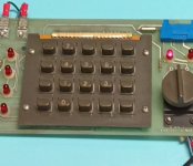
I have a spare console & M7859.
The spare console appears to be mostly working except some of the keypad keys are difficult to operate - the Zero key is really bad and takes several presses to register.
Has anyone tried to disassemble and clean the keypad? Are there any hidden dragons there?
The spare M7859 is not working. The 8008 gets a clock which is about 700 kHz as opposed to the 1 MHz on the good M7859. I have no great ideas how to debug and fix this and would appreciate any help or suggestions.

KM11
Experienced Member
The ribbon connection seems to be one of the more common failure points of the keypad. You may find the video link below interesting (particularly around 20:00), although I should point out that this fellow appears to be learning as he goes (no criticism intended), so some things he says may be a bit misleading or inaccurate.
thunter0512
Veteran Member
I have a spare console & M7859.
The spare M7859 is not working. The 8008 gets a clock which is about 700 kHz as opposed to the 1 MHz on the good M7859. I have no great ideas how to debug and fix this and would appreciate any help or suggestions.
It turned out that the 8008 CPU was stuck in HALT mode after power on.
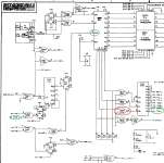
The root cause of the problem was a dead E24 a DS8837 used to drive the inputs into E23 a 7442 demultiplexer used to decode the state S0/S1/S2 signals into individual active low signals.
While the 8008 correctly output the state signals for the HALT state it was in (S0/S1/S2 = 1/1/0), the output of E23 showed it to be in state T4 with pin 1 active low (because E24 fed it 0/0/0 rather than 0/0/1).
This prevented the initialisation logic to run and generate the interrupt to get the 8008 out of its HALT state.
Here is the schematic with the faulty part highlighted in red and a few key signals highlighted in green (click to see full size):
Fist I unsuccessfully tried Jerry Walker's suggested way of removing ICs using solder wick. This did not work for me and I stopped before I damaged any pads or the PCB.
Instead I used a narrow side cutter to cut all pins of E24 close to the body of the IC. I keep this side cutter just for this purpose.
Using a soldering iron set to 330 degrees C and needle nose tweezers I carefully removed all pins individually.
Finally I sucked all the solder from the holes with my vacuum desoldering setup.
This approach is relatively gentle but sacrifices the IC.
Rather then soldering the replacement 8837 directly I used a socket.
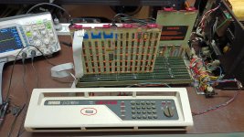
Here is a photo of the running front panel with the repaired M7859. I have highlighted the replacement IC in its socket and the removed IC sitting on the font panel (click to see full size):
antiquekid3
Veteran Member
This is my favored approach as well if I know the chip is dead. I also like a good vacuum desoldering station if I'm trying to preserve the chip. I find wick to be very finicky, and as you point out, you certainly risk damaging the pads.Instead I used a narrow side cutter to cut all pins of E24 close to the body of the IC. I keep this side cutter just for this purpose.
Using a soldering iron set to 330 degrees C and needle nose tweezers I carefully removed all pins individually.
Finally I sucked all the solder from the holes with my vacuum desoldering setup.
This approach is relatively gentle but sacrifices the IC.
Nice work!
cchhrriiss11
Experienced Member
Great repair technique and nice ceramic 8008... there's one on both of my M7859's as well - in-fact, that's where I got my profile photo from.It turned out that the 8008 CPU was stuck in HALT mode after power on.
The root cause of the problem was a dead E24 a DS8837 used to drive the inputs into E23 a 7442 demultiplexer used to decode the state S0/S1/S2 signals into individual active low signals.
While the 8008 correctly output the state signals for the HALT state it was in (S0/S1/S2 = 1/1/0), the output of E23 showed it to be in state T4 with pin 1 active low (because E24 fed it 0/0/0 rather than 0/0/1).
This prevented the initialisation logic to run and generate the interrupt to get the 8008 out of its HALT state.
Here is the schematic with the faulty part highlighted in red and a few key signals highlighted in green (click to see full size):
View attachment 1264372
Fist I unsuccessfully tried Jerry Walker's suggested way of removing ICs using solder wick. This did not work for me and I stopped before I damaged any pads or the PCB.
Instead I used a narrow side cutter to cut all pins of E24 close to the body of the IC. I keep this side cutter just for this purpose.
Using a soldering iron set to 330 degrees C and needle nose tweezers I carefully removed all pins individually.
Finally I sucked all the solder from the holes with my vacuum desoldering setup.
This approach is relatively gentle but sacrifices the IC.
Rather then soldering the replacement 8837 directly I used a socket.
Here is a photo of the running front panel with the repaired M7859. I have highlighted the replacement IC in its socket and the removed IC sitting on the font panel (click to see full size):
View attachment 1264373
-Chris
Michael Robinson
Member
This is my favored approach as well if I know the chip is deadInstead I used a narrow side cutter to cut all pins of E24 close to the body of the IC. I keep this side cutter just for this purpose.
Using a soldering iron set to 330 degrees C and needle nose tweezers I carefully removed all pins individually.
Finally I sucked all the solder from the holes with my vacuum desoldering setup.
This approach is relatively gentle but sacrifices the IC.
I concur! I've done this approach many times and even recall seeing it detailed in a DEC maintenance manual somewhere.
I only got in trouble once, but that was because I stole my dedicated side cutters from our bathroom without informing the other inhabitants of my house... the cutters were originally sold as cuticle cutters. They have very sharp and narrow jaws, which I prefer over some of the other options.
I've never mastered solder wick for delicate work but not for lack of trying...
thunter0512
Veteran Member
In the past few days I have quietly worked on the remaining spare M7859 Programmer's Console controller board.
The board must have been through something traumatic as E56 had exploded (click to see full size):
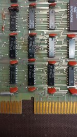
E56 is a DS8641N a Quad Unified Bus Transceiver.
The explosion has taken out a small section of track which I repaired after removing the IC and replacing it with a socketed IC salvaged from a scrap board.
I am quite successful pulling ICs from scrap DEC boards with my vacuum desoldering station because I don't have to try preserve the pads.
With DEC boards and "bent pin manufacturing" I can preserve IC or board, not both.
Here is a photo showing the whole board before repair (click to see full size):
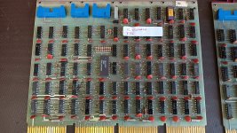
After replacing E56 and repairing the damaged track surprisingly the board was somewhat functional. The left-most two digits of the display were blank.
This turned out to be caused by a faulty E57 a 74175 a Quad D-type Flip-Flop.
It is located next to and connected to the exploded E56 so the damage is not surprising.
After replacing E57 with a socketed version of a 74175 the display worked.
Unfortunately the board was not yet fully functional - far from it.
The recommended self-test is to load a value into the on-board Switch Register and then examine it at Unibus address 777570.
This self-test resulted in a Bus Error.
I probed the address decode around E60/E40/E32 and it appeared that several address lines were garbage by the time they got to the decode logic.
The first problem with the addresses was that E51 (another 74175) pin 11 (KY7 EN AR -> BUS L) was stuck low - always enabled.
This meant that whatever happened on the address register pins was transparently reflected on the Unibus address lines.
What should happen is that the contents of the address registers is only presented on the Unibus address lines when the the associated Bus Transceivers are enabled.
Otherwise the keyboard and display scan activity makes it onto the Unibus address lines which is not good.
After replacing E51 (74175) with a socketed version, the Bus Transceivers got good enables.
When probing the address lines, triggering on the now functional enable signal (pin 9) of every DS8641 Bus Transceiver, I noticed that several output bits were not following their input. I ended up replacing all remaining DS8641 Bus Transceivers associated with the 18-bit Unibus address lines with socketed versions of the ICs salvaged from a unrelated scrap board. So that was E61, E65, E55 and E50. I already had replaced the exploded E56.
Finally I could see the addresses I tested with (777777 and 000000), except address bits 8 and 9 which did not show valid TTL HIGH levels on pins 3 and 6 of E65.
The signals were pulled towards ground and only reached about 1.6V.
I pulled the now socketed E65 DS8641 and re-tested it. It worked perfectly. Hmmm ...
The associated signals were "KY6 BB A08 H" and "KY6 BB A08 H".
These fed into the previously mentioned address decode logic but also into E70 a DM8093 Quad Buffer.
I was reluctant to pull E70 with my vacuum desoldering station to preserve the IC as this always risks damage to the board.
Instead I cut pin 2 of E70 ("KY6 BB A08 H").
Unfortunately the signal was still being pulled towards ground.
I patched up the cut pin 2 of E70.
This left only the address decode logic as the cause of the invalid TTL levels of signals "KY6 BB A08 H" and "KY6 BB A08 H".
Specifically E60 a 13 input NAND gate 74S133.
After cutting pin 12 of E60 which receives signal "KY6 BB A08 H" the signal became good and was no longer pulled towards ground.
I replaced E60 with a socketed version of a salvaged 74S133.
Finally when I tried the self-test (examine the Switch Register at Unibus address 777570) I saw a valid address decode triggering signals "BUS SSYN L" and "KY4 EN DB -> BUS L" which place the data onto the Unibus data lines and starts the sampling of the data on the bus.
I no longer got a Bus Error - which was good, but the SR value read back had bit 1 always zero. So a value 777 read back as 775.
A few more minutes of probing signals showed the remaining culprit being E9 another faulty 74175 implementing Switch Register bits 0 - 3.
I replaced E9 with a socketed and salvaged version, but in my excitement cut out E10 (another 74175) first. Oh well - collateral damage.
So now both E9 and E10 are socketed with salvaged ICs.
Finally the M7859 Programmer's Console controller board Self Test worked as it meant to.
Here is a photo of the fully repaired board - note the many sockets ((click to see full size):
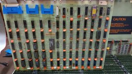
I already had a working spare board, but was determined to make this "exploded" board work too.
The board must have been through something traumatic as E56 had exploded (click to see full size):

E56 is a DS8641N a Quad Unified Bus Transceiver.
The explosion has taken out a small section of track which I repaired after removing the IC and replacing it with a socketed IC salvaged from a scrap board.
I am quite successful pulling ICs from scrap DEC boards with my vacuum desoldering station because I don't have to try preserve the pads.
With DEC boards and "bent pin manufacturing" I can preserve IC or board, not both.
Here is a photo showing the whole board before repair (click to see full size):

After replacing E56 and repairing the damaged track surprisingly the board was somewhat functional. The left-most two digits of the display were blank.
This turned out to be caused by a faulty E57 a 74175 a Quad D-type Flip-Flop.
It is located next to and connected to the exploded E56 so the damage is not surprising.
After replacing E57 with a socketed version of a 74175 the display worked.
Unfortunately the board was not yet fully functional - far from it.
The recommended self-test is to load a value into the on-board Switch Register and then examine it at Unibus address 777570.
This self-test resulted in a Bus Error.
I probed the address decode around E60/E40/E32 and it appeared that several address lines were garbage by the time they got to the decode logic.
The first problem with the addresses was that E51 (another 74175) pin 11 (KY7 EN AR -> BUS L) was stuck low - always enabled.
This meant that whatever happened on the address register pins was transparently reflected on the Unibus address lines.
What should happen is that the contents of the address registers is only presented on the Unibus address lines when the the associated Bus Transceivers are enabled.
Otherwise the keyboard and display scan activity makes it onto the Unibus address lines which is not good.
After replacing E51 (74175) with a socketed version, the Bus Transceivers got good enables.
When probing the address lines, triggering on the now functional enable signal (pin 9) of every DS8641 Bus Transceiver, I noticed that several output bits were not following their input. I ended up replacing all remaining DS8641 Bus Transceivers associated with the 18-bit Unibus address lines with socketed versions of the ICs salvaged from a unrelated scrap board. So that was E61, E65, E55 and E50. I already had replaced the exploded E56.
Finally I could see the addresses I tested with (777777 and 000000), except address bits 8 and 9 which did not show valid TTL HIGH levels on pins 3 and 6 of E65.
The signals were pulled towards ground and only reached about 1.6V.
I pulled the now socketed E65 DS8641 and re-tested it. It worked perfectly. Hmmm ...
The associated signals were "KY6 BB A08 H" and "KY6 BB A08 H".
These fed into the previously mentioned address decode logic but also into E70 a DM8093 Quad Buffer.
I was reluctant to pull E70 with my vacuum desoldering station to preserve the IC as this always risks damage to the board.
Instead I cut pin 2 of E70 ("KY6 BB A08 H").
Unfortunately the signal was still being pulled towards ground.
I patched up the cut pin 2 of E70.
This left only the address decode logic as the cause of the invalid TTL levels of signals "KY6 BB A08 H" and "KY6 BB A08 H".
Specifically E60 a 13 input NAND gate 74S133.
After cutting pin 12 of E60 which receives signal "KY6 BB A08 H" the signal became good and was no longer pulled towards ground.
I replaced E60 with a socketed version of a salvaged 74S133.
Finally when I tried the self-test (examine the Switch Register at Unibus address 777570) I saw a valid address decode triggering signals "BUS SSYN L" and "KY4 EN DB -> BUS L" which place the data onto the Unibus data lines and starts the sampling of the data on the bus.
I no longer got a Bus Error - which was good, but the SR value read back had bit 1 always zero. So a value 777 read back as 775.
A few more minutes of probing signals showed the remaining culprit being E9 another faulty 74175 implementing Switch Register bits 0 - 3.
I replaced E9 with a socketed and salvaged version, but in my excitement cut out E10 (another 74175) first. Oh well - collateral damage.
So now both E9 and E10 are socketed with salvaged ICs.
Finally the M7859 Programmer's Console controller board Self Test worked as it meant to.
Here is a photo of the fully repaired board - note the many sockets ((click to see full size):

I already had a working spare board, but was determined to make this "exploded" board work too.
thunter0512
Veteran Member
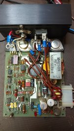
After gaining a good understanding of the operating principle of the H7441 5V 32A supply (see Theory of operation of H7441 regulator), I finally repaired my faulty H7441. Thanks to those who described the circuit so that even I understood it.
The main problems was a faulty E3 an LM301 op-amp which spuriously signalled "over-current" and shut down the supply via Q7. I replaced it with a new socketed IC.
The other was the corroded Drain pin of Q9 a 2N5433 FET were the lower part of the pin disintegrated when I touched it with the scope probe. Unfortunately the 2N5433 is no longer made and is only available at silly prices on Ebay, so for now I just patched up the pin with a wire as there was enough of the pin left to solder onto. I have ordered a few from France. I suspect there are suitable substitutes which are still made and available.
I have also replaced two out-of-spec resistors (R20 and R32).
Here are a few photos (click to see full size) :
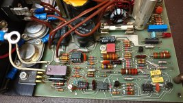
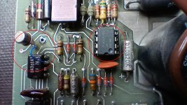


thunter0512
Veteran Member
My spare 5411086 (+15V switch mode supply and AC low & DC low sensing) asserted "AC low" and "DC low" for 2 - 3 minutes after power-on before de-asserting both signals.
This was very visible on the 11/34 programmers console as the display is off with "DC low" asserted. After 2 - 3 minutes the display would come and go for another 5-10 seconds before it stabilised.
While checking the signals the gates of the 2N5433 JFETs (Q14, Q15, Q17 and Q18) had a marginal signal of only about -4V where the datasheet specifies a Vgs(off) range between -3V and -9V.
It appeared that as the JFETs warmed up the Vgs(off) shifted a bit so they turned off and "AC low" and "DC low" de-asserted. These JFETs are very noisy as they change from on to off.
At first I suspected Q10 and Q19 (MPSA05 - NPN transistors) based on in-circuit measurements.
Once I removed both I confirmed Q19 (used for "AC low") was faulty, but Q10 (used for "DC low") was perfectly fine. I replaced both with PN100 general purpose transistors for now until I get the correct parts from the US.
Of course "DC low" and AC low" were still mis-behaving while the board was cold, so my hunt continued.
The two red LEDs showing the status of "AC low" and "DC low" were rather dim, so I focused on the two differential amplifiers used for the sensing.
As I probed the signals I realised that the reference voltage created by the two 5.1V Zeners (D13 and D14) was only about 5.2V rather than the expected 10.2V.
It turned out D13 was a dead short. I replaced both D13 and D14 with new Zeners and now both "AC low" and "DC low" work as expected.
Here is the schematic (click to see full size) :
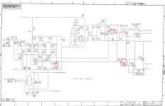

thunter0512
Veteran Member
With some spare PDP-11/34 boards, fully working power supplies and fully working 11/34 programmer's console I have finally assembled a system that appears to mostly work.
The boards used are:
M7266 (CPU)
M7265 (CPU)
M7847-BJ (16 kW MOS memory)
M7859 (console controller)
M7856 (serial port)
M9312 (boot/terminator)
all empty slots have the small grant continuity boards in position D.
The M9312 is configured to boot into the serial console.
The serial console works as documented except that the prompt character is "@" instead of the documented "$".
To get this far means that lot of the system is working and executing PDP-11 code, but unfortunately not everything.
According to the manual the system does a basic CPU self test before entering the serial console mode.
Some extended CPU self test is executed when you attempt to boot some non-existing device.
My M9312 has a boot ROM labelled 758A9 which supports booting from various magnetic tape via the serial console boot command "MT".
When I type "MT" in the serial console the system performs this "extended" CPU test and then halts at address 165774.
Don North's nice "M9312 PROM files" page on GIThub ( https://ak6dn.github.io/PDP-11/M9312/ ) is very helpful as it provides the PROM images, but also the source and listing files for all known M9312 PROMs.
Looking at the 248F1 serial console PROM listing around address 165774 it becomes clear that the system halted because of a memory error. The fault location is in R0 and the "bad" data is in R4.
Using the programmer's console I examined the 11/34 registers at addresses 777700 to 777707:
R0 was 020042
R4 was 000000
The diagnostics code appears to size memory and then in a loop write each location's address into that location.
In a following loop it then adds the negated address into each location and tests that the data at that location is now zero.
If this fails the current address is saved to R0 and the "bad" data (after the add) is saved to R4 before halting.
In this case R4 is 000000 which is what was expected, so the extended self test shouldn't have halted!
I tried another M7847-BJ memory board and it too failed in a similar way at a different address (36110), but with a plausible "bad" data value of 004000 which indicates a one-bit failure.
Any ideas of what might be going on and what debugging or diagnostics I should try next?
I don't have the 760A9 PROM (in my M9312) which supports the ASR33 low-speed reader - boot command "TT" to boot diagnostics from paper tape (if they even exist).
Maybe I could burn Don North's hex file into a PROM, but first would need to find a suitable PROM. I do have a burner which should program most bipolar PROMs.
I would appreciate any advice and/or suggestions.
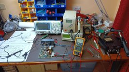
Here is a photo of my PDP 11/34 debug setup sitting on my work bench/trolley showing the halted state and location after trying to boot from "MT" (click to see full size) :
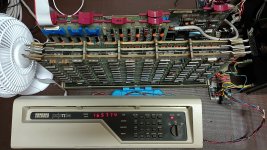
Thanks
Tom
The boards used are:
M7266 (CPU)
M7265 (CPU)
M7847-BJ (16 kW MOS memory)
M7859 (console controller)
M7856 (serial port)
M9312 (boot/terminator)
all empty slots have the small grant continuity boards in position D.
The M9312 is configured to boot into the serial console.
The serial console works as documented except that the prompt character is "@" instead of the documented "$".
To get this far means that lot of the system is working and executing PDP-11 code, but unfortunately not everything.
According to the manual the system does a basic CPU self test before entering the serial console mode.
Some extended CPU self test is executed when you attempt to boot some non-existing device.
My M9312 has a boot ROM labelled 758A9 which supports booting from various magnetic tape via the serial console boot command "MT".
When I type "MT" in the serial console the system performs this "extended" CPU test and then halts at address 165774.
Don North's nice "M9312 PROM files" page on GIThub ( https://ak6dn.github.io/PDP-11/M9312/ ) is very helpful as it provides the PROM images, but also the source and listing files for all known M9312 PROMs.
Looking at the 248F1 serial console PROM listing around address 165774 it becomes clear that the system halted because of a memory error. The fault location is in R0 and the "bad" data is in R4.
Using the programmer's console I examined the 11/34 registers at addresses 777700 to 777707:
R0 was 020042
R4 was 000000
The diagnostics code appears to size memory and then in a loop write each location's address into that location.
In a following loop it then adds the negated address into each location and tests that the data at that location is now zero.
If this fails the current address is saved to R0 and the "bad" data (after the add) is saved to R4 before halting.
In this case R4 is 000000 which is what was expected, so the extended self test shouldn't have halted!
I tried another M7847-BJ memory board and it too failed in a similar way at a different address (36110), but with a plausible "bad" data value of 004000 which indicates a one-bit failure.
Any ideas of what might be going on and what debugging or diagnostics I should try next?
I don't have the 760A9 PROM (in my M9312) which supports the ASR33 low-speed reader - boot command "TT" to boot diagnostics from paper tape (if they even exist).
Maybe I could burn Don North's hex file into a PROM, but first would need to find a suitable PROM. I do have a burner which should program most bipolar PROMs.
I would appreciate any advice and/or suggestions.
Here is a photo of my PDP 11/34 debug setup sitting on my work bench/trolley showing the halted state and location after trying to boot from "MT" (click to see full size) :

Thanks
Tom
AK6DN
Veteran Member
...
Don North's nice "M9312 PROM files" page on GIThub ( https://ak6dn.github.io/PDP-11/M9312/ ) is very helpful as it provides the PROM images, but also the source and listing files for all known M9312 PROMs.
...
Looking at the 248F1 serial console PROM listing around address 165774 it becomes clear that the system halted because of a memory error. The fault location is in R0 and the "bad" data is in R4.
...
Maybe I could burn Don North's hex file into a PROM, but first would need to find a suitable PROM. I do have a burner which should program most bipolar PROMs.
...
I would appreciate any advice and/or suggestions.
...
Thanks
Tom
Years ago I was able to get a box of 1000pcs of 82S129 NOS parts that are suitable for the M9312 device boot prom. They are 256x4 instead of 512x4 that DEC used,
but for some reason DEC only used the low half and left the other half blank. Anyway the .hex files on my site can be directly programmed in the 256x4 parts and plugged
directly into the M9312 (or 11/44 or 11/24 ...) etc sockets.
SO if you need some blank devices HMU. Shipping to the other side of the world (I have shipped to you before...) is expensive but I'm here if you can't find anything locally.
Or anyone else that matter that needs either blank or programmed boot devices (I have a bipolar prom programmer as well).
$5 each programmed, $3 each blank. Tube of 25pcs blank $50 per tube. Shipping extra.
Don
PS: I also use my ZZ device in my 11/34 M9312 which is a fake device that runs the console prom resident diagnostics continuously, useful as a very basic system sanity check.
Last edited:
thunter0512
Veteran Member
Hmmm - I looked a bit more into what types of bipolar PROMs are used in the PDP-11/34 planning to get a few blank ones of each.
It appears DEC used a mix of PROMs including 32 x 8, 256 x 4, 512 x 4 with both tri-state and open-collector outputs.
This lack of standardisation makes it a bit harder to acquire "stock" of all types.
It appears DEC used a mix of PROMs including 32 x 8, 256 x 4, 512 x 4 with both tri-state and open-collector outputs.
This lack of standardisation makes it a bit harder to acquire "stock" of all types.
AK6DN
Veteran Member
Hmmm - I looked a bit more into what types of bipolar PROMs are used in the PDP-11/34 planning to get a few blank ones of each.
It appears DEC used a mix of PROMs including 32 x 8, 256 x 4, 512 x 4 with both tri-state and open-collector outputs.
This lack of standardisation makes it a bit harder to acquire "stock" of all types.
32x8, 256x4, 256x8, 512x4, 512x8, 1Kx4 were all common standard BPROM sizes in those days, and DEC would optimize the
number of inputs/outputs and type (OC vs TS) to the particular application. Using only one type (ie, 256x8) as a catchall
was not cost effective when all devices were equally available.
thunter0512
Veteran Member
I installed PDP11GUI (thanks Joerg) and it's built-in memory test passes.
After loading the paper-tape BASIC with PDP11GUI I get a READY prompt. After entering two lines of a BASIC program my PDP-11/34 halts.
My Google searches for PDP-11/34 diagnostics yields a confusing mix of stuff, but finally I stumble across Joerg's Diagnostics Database which again is rather confusing.
Via PDP11GUI I loaded and ran the "Basic Instruction Test" at:
It almost immediately halts at address 26136 without any output on the console terminal.
Unfortunately I am not entirely sure what the associated program listing is, but it may be:
According to that (possibly mis-matched) listing it halted because it "trapped thru location 10". The 11/34 Processor Handbook says that traps through location 10 are caused by "reserved instructions".
Now what? I am confused and somewhat overwhelmed. I am not even sure that the program listing matches the diagnostic program binary.
My previous adventures with the two PDP-8/e machines were made a bit easier by a nice consistent set of diagnostics and associated program listings from Vince's website.
I have not yet found the same resource for the 11/34.
MattisLind
Veteran Member
The diags are just printing out when successfully run a full iteration (or send a BELL). If there is a HALT then you need to track down what happened using the listing.
You say that it halts at address 26136. The halt instruction is then on 26134. It matches the listing. So it took a 010 trap. You need to look at the stack where it was prior to the trap.
BTW. This is the test you can run from XXDP, but all .BIC files are standard absolute binary files that can be loaded using Jörgs PDP11GUI.
thunter0512
Veteran Member
I don't know how XXDP would help as I would still need the diagnostic listing to understand the problem causing the HALT?Would XXDP be of any use here if you can't find the proper 11/34 diag and listing? Of course the proper 11/34 diagnostics would be best but this might help.
My current very limited understanding is that XXDP is a platform to launch diagnostics from - like a mini-OS for diagnostics.
I have the suspicion that my problems are caused by bad memory. After the FKAA diagnostics failed PDP11GUI found a pattern of locations which had wrong values. I had no chance yet to understand that pattern.
thunter0512
Veteran Member
I don't yet fully understand how the stack operates on the PDP-11, but I looked up R6 which is 474. When I examine 474 I see the following:The diags are just printing out when successfully run a full iteration (or send a BELL). If there is a HALT then you need to track down what happened using the listing.
You say that it halts at address 26136. The halt instruction is then on 26134. It matches the listing. So it took a 010 trap. You need to look at the stack where it was prior to the trap.
BTW. This is the test you can run from XXDP, but all .BIC files are standard absolute binary files that can be loaded using Jörgs PDP11GUI.
474: 20044
476: 357
480: 12737
482: 26002
The manual is a bit vague about which is the saved PSW and which is the saved PC, but i suspect that PC=20044 and PSW=357 assuming a pre-decrement of R6 for each push.
Assuming that the trap occurs after the PC has been incremented, the faulting instruction (according to the possibly mis-matched listing) is "+CLN!CLV" at location 20042 which are condition code clear instructions combined into one word.
I will re-run this test tomorrow with a fresh brain and try to confirm that the suspected fault location actually contains these instructions.
As I wrote in #58 I have a suspicion that the memory is not healthy as the M9312 built in memory diagnostics fails at location 20042 which is right next to 20044 which I found on the TRAP 10 stack.
I don't have a M7850 Parity Controller - is that something I must have or is it optional with my M7847-BJ memory? Too much works for the missing M7850 to be the cause my problems.
AK6DN
Veteran Member
For my 11/34 I have built a couple of XXDP diagnostics disks located here: https://ak6dn.github.io/PDP-11/TU58/ that I use with my TU58 emulator.
1134_1.DSK (and associated listing .TXT) and 1134_2.DSK (and .TXT) are the TU58 images.
Typically I run from the XXDP prompt using the 'chain' feature to run a quick verify pass of the diagnostics.
'C TEST' to run all the .BIC files on the disk, 'C FKAAC0' (etc) to run a specific .BIC diagnostic for one pass and return to the monitor.
The .BIN versions are load and run only 'R FKKAB0' (etc) and will run continuously until the system is halted and rebooted to XXDP.
Also I have a memory tester that I wrote MEMX.BIN on the 11XX_9.DSK image (R MEMX) that does a comprehensive test of the full memory using relocation.
Also in https://ak6dn.github.io/PDP-11/RX02/ there are corresponding RX02 XXDP images files to the above TU58 images for those that
have an RX02 emulator you can put all those .RX2 image files on the microSD card and boot each XXDP file in a similar fashion to run the diagnostics.
Last edited:
