• Please review our updated Terms and Rules here

PET 3016 memory upgrade

I noticed on the layout schematic there is this thing called Detail B which shows alternative track layouts for some configurations. Do I need to alter them for 4116 configurations? There are three positions on the board labelled Detail B. They are currently not cut (refer to the detail B diagram) attached.

As I read it, you only need this for 8k models, but I thought I'd better check.
 

Attachments

  • detail B.JPG
    detail B.JPG
    14.8 KB · Views: 1
  • 16K shunt config.JPG
    16K shunt config.JPG
    16.6 KB · Views: 1
Some progress, I think.

I discovered that the /RAS line on U18 wasn't connected. It is connected to the pad on the underside of the board, but the track is on the top side and the top side pad isn't connected. I put in a temporary link from the /RAS via to the IC's /RAS pin (4) and rebooted. Now, instead of a single character on the screen halfway down, there is a line of junk on the very first line that is 32 characters wide. This is a bit random. I turned it off then on again and this time I got some junk that also includes "READY" and what looks like a line of assembly - is it in the monitor?

it says:

Code:
READY. @@@@@@@@@//LOAD
;   007C E62E BC  AC XR YR SP

..with the @ signs represented on screen as random graphics characters.

Another reboot attempt gave me various random characters written to the screen in three lines (all consecutive). I pressed STOP and it said BREAK; on ENTER it said PRESS PLAY ON TAPE. But it won't actually get to the BASIC prompt. I suspect memory corruption somewhere - need to check all the other top pads for continuity with the RAM chip legs. Retries give random variations on the same theme.
 
Last edited:
Some progress, I think.
Yes, keep finding bad RAM connections. Concentrate on the "I" row of chips as they are needed to boot (low address RAM). It is trying to come up but needs good zero page RAM (address 0000 - 0100) and stack area (0100-0200). You are close!
 
Hmmm, CAS0 and CAS1 are fixed high, that's not right.

Using the other schematics on Zimmers, I traced the line back to G7. The inputs weren't pulsing either, so I followed that back to H4, a 74LS157 quad 2 to 1 multiplexer. It has 4 outputs, Y1-4. Y4 (pin 12) wasn't pulsing - I can't remember now if any others were. Again, tracing back to H3 (74LS164 shift register), I measured pulses on all its outputs QA-QH. So I figured that H4 was zapped.

I pulled H4 out and fitted a socket. Scavenging a 74LS157 from one of the dead Spectrums, I fitted it, checked continuity (all good) and powered up.

Same thing. I was thinking I'd been mistaken, but I checked the outputs anyway. All good and pulsing. I returned to RAM Bank1 to check CAS and RAS lines. All pulsing now, so that bit at least is fixed.

Then (for some reason) I was checking the data lines, and I discovered that one of the RAM chips had no output, so I whipped it out and slotted in a spare. It fired up, booted correctly and showed 16k of memory, huzzah!

So now, what about the purpose of all this hackery, the 32k upgrade? I checked the shunts - I thought all I had to do was link H and I'd be sorted. So, one blob of solder and 8 4116 chips later, I'm firing it up again. Ooops! Got the garbage screen, and it's not clearing. Better recheck those shunts - I should have opened M as well! I opened it up and again checked they were correct - a bit more carefully this time. All good.

So, finally, I powered it up again.

The screen shows

Code:
### COMMODORE BASIC ###

 31743 BYTES FREE

READY.
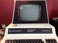
:clap2:

WHO'S THE DADDY??? ME!!
 
Last edited:
image.jpg


A big thank you to everyone who offered advice, and if your PET is sick, you can fix it with only basic equipment (multimeter, logic probe, soldering iron, solder sucker) and consumables (solder plus whatever chips need replacing, and sockets for the chips). The key is determination, and to take a break whenever you feel frustrated.

And of course, major thanks to Bo Zimmerman and his great resource Zimmerman.net, where all the schematics are.

Cheers!

JonB

:toast:
 
and if your PET is sick, you can fix it with only basic equipment (multimeter, logic probe, soldering iron, solder sucker) and consumables (solder plus whatever chips need replacing, and sockets for the chips). The key is determination, and to take a break whenever you feel frustrated.

Well done! And yes, you're right, determination (and some method) is what you really need with this old beasts.... It took me *12 years* to fix my 3032 :D
 
and if your PET is sick, you can fix it with only basic equipment (multimeter, logic probe, soldering iron, solder sucker)

Congratulations on fixing your PET computer. I'm also glad you left off the equipment list the 1200W heat gun and the vacuum cleaner. I would guess that the H4 chip you had to replace got "too close" to your hair dryer. And if you had taken 2 minutes to continuity check the shunts, you would have found most of your problems. You did a really good job of spotting the lack of output on the bad RAM chip which showed good troubleshooting skills. Overall, good job!
 
I did continuity check the shunts, both times, but I'd misread the 32k setting of M=open so I had left it closed when I first installed Bank 2.

In summary, the problems were:

* No /CAS at all - caused by the defective multiplexer chip.
* No /RAS to one RAM chip in Bank 1 - caused by a broken track (I assume; I fixed it with a wire for now).
* No output to one data line of one Bank 1 RAM chip - caused by the chip being defective (and after I'd tested it).

Actually, the heat gun was useful when I was scavenging the multiplexer from the Spectrum PCB. I tried to desolder the pins with my sucker but couldn't clear them. Going to have to look into that... but for now I'd say one can use a heat gun to remove chips you want to use from a discardable board if care is taken. If you want to keep the board, you need even more care; you should always desolder the pads with an iron and solder sucker. No more vacuum cleaners!

:)
 
Last edited:
Rats! Turned it on this morning and it's reporting 15391 bytes free.

Out with the logic probe / multimeter again.... :D

Edit: Took all the RAM from Bank 2 and the 74LS157 (UH4) is dead again. No /CAS. UG7 that feeds it is OK. Also some anomalies on the address bus. Very odd! New 157 ordered..
 
Last edited:
Edit: Took all the RAM from Bank 2 and the 74LS157 (UH4) is dead again. No /CAS. UG7 that feeds it is OK. Also some anomalies on the address bus. Very odd! New 157 ordered..

UH4 is close to the overcooked PCB heat gun area. Check all the traces there for intermittent connections.

Before taking the RAM chips out, perhaps you should have tried to PRINT PEEK( 15391 + 1025). The answer when convert to hex and compared to the test patterns of $55 (01010101) or $AA (10101010) might have indicated what bits are acting up. But I think you are on the right trail. Good hunting.
-Dave
 
I have ordered some 157s. As I said, all the other outputs are working, and I tested at the IC leg, not the board. I'm fairly sure the IC has popped. Question is, why? I can dig the first one going (probably got too hot), but a second one? And on the same output? Seems a bit too much of a coincidence to me - there must be something else that's causing it. So I'd better do as you suggest - although I did check traces before discovering the zapped 157. Can't hurt to do it again!

Interesting that although it's jumpered for 32K it can run at 16. But then it's MS BASIC in disguise, and I'm pretty sure that checks for RAM at start-up and adjusts the free RAM accordingly. At least, it does on my UK101 clone (Ohio Superboard clone sold in the UK). Err, so that's a clone of a board that's a clone of a board. :D
 
I have ordered some 157s. As I said, all the other outputs are working, and I tested at the IC leg, not the board. I'm fairly sure the IC has popped.

If one of the 157 decoder inputs is open, then one or more of the outputs could appear dead as it never gets the correct input pattern to activate.
 
Hmmm, thanks. Gotta confess the actual function of some of these 74 series chips is a bit beyond me sometimes. Noob is all. I'll get there.

 
Isn't that just a compendium of data sheets?

I have here a copy of "High Speed CMOS logic data" which is a Motorola publication, and it does explain the 157 function (HC, but this is an electrical difference, not a functional difference). It says, in effect, that the chip takes 4 inputs (basically, a nibble) and switches them between two sets of four outputs; the switch being implemented by the select line. It's like a four gang switch, so you can route your four inputs to one of two sets of four outputs.
 
Last edited:
Right.. one new multiplexer later, and we're up and running. I think there's a sort of "half fail" state here that means the PET only sees the first bank, but I'm not 100% sure. The temporary RAS wire on UI8 was a bit loose too, so perhaps that is why it was reporting intermittent memory sizes. Must fix it, but for now it is working fine. I entered the memory test program from PET Revealed and ran it for 2048-16383 (bank 1) and 16384-32767 (bank 2) and it reported zero memory faults. Mind you I'm not sure it really did test all the memory. It says it only does the bottom 8k, but then why does it allow you to set a range?

Hmm, more testing coming.. :)
 
Ah. I ran it against the video RAM - 32768 - 34815 and it filled the screen, so the parameters work.

Interesting - the screen memory addresses appear to be duplicated. 1 screen = 1K but there is 2K in the memory map for it. The second K maps onto the first, from the looks of it. Would be nice if we could use that second K for, oh I dunno, screen attributes like colours.. ;) Yeah I know it's been done, but on a CRTC PET...
 
Back
Top