• Please review our updated Terms and Rules here

PET 3032 garbage screen problem

Fran

Experienced Member
Joined
Jan 27, 2019
Messages
69
Location
Spain
Hi
My pet 3032 has the problem of garbage screen
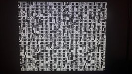
20190824_133701.jpg

I have checked all pcb voltages and they are correct. + 5V, + 12V, -5V and + 9V, according to the diagrams:
http://www.zimmers.net/anonftp/pub/cbm/schematics/computers/pet/2001N/320349-1.gif
to
http://www.zimmers.net/anonftp/pub/cbm/schematics/computers/pet/2001N/320349-8.gif

I have checked the ram and roms with the http://blog.tynemouthsoftware.co.uk/2015/09/commodore-pet-rom-ram-replacement-boards.html and they are ok.
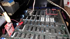
20190824_140644.jpg

When boot with replacement boards the same

The difference is that if I press the reset button on the replacement board it loads the basic screen but with garbage, whether I use the board roms/rams or replaced roms/rams
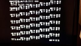
20190824_141100.jpg

Help me please
 
If RAM and ROMs are ok (but I doubt they can be safely tested from a daughterboard, having made my own daughterboard too), then this looks like a data (or even address/decode) conflict with some other parts. It could be an I/O chip or maybe a data bus transceiver (74LS244) or it might be an address bus buffer failing or any part of address decoding logic faiiling. Do you have an oscilloscope or logic probe?
Frank IZ8DWF
 
Yes, I have an osilloscope. What should i check? What chips? What pins? What values?
 
Yes, I have an osilloscope. What should i check? What chips? What pins? What values?

I agree with Frank that because of the alternating inverse video, and repeating patterns, etc. there may be an addressing logic issue rather than bad RAM. Can someone post the info about making a simple NOP Generator so that the address lines can be easily traced?
 
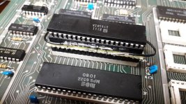
Here's the wiring; use a 40-pin socket, bend out the appropriate pins and run the wires around the outside so you can insert the 6502.

6502_NOPpcb-ad5f77f0e6c0439f8e08cece619c407e


An interesting blog, although the link to the instructions seems to be dead:

http://www.8bit-homecomputermuseum.at/repair/bluepet/bluepet.html
 
Yes, that's it. The trick is to use two sockets so that the NOP instruction pattern (1110 1010) is connected to the CPU chip only on the top socket, and the data lines (D7 thru D0) pins 26 thru 33 are open to the board circuitry on the bottom socket. In that way the CPU will happily execute NOPs all day while incrementing the address lines from $0000 to $FFFF. The CPU will then roll over to zero and start again. With a scope you can follow the square waves on the address lines. A0 will have the highest frequency of about 500 KHZ, A1 half of that, and A2 half of A1. If you spot something not in that pattern, you have found the problem. Note however that the RAM address inputs are multiplexed with the dynamic RAM refresh logic so it gets a little messy there. Hopefully with this method you will spot a bad buffer or whatever.

Also I would look at the eight data lines at the board for shorted or open signals. Note that the $E900-EFFF space is not allocated and there will be tri-state there where no device is selected. You can use SEL E to help sync that period and ignore.
 
With a nop generator under the 6502, I'd first check each address going through UC3 and UB3:

http://www.zimmers.net/anonftp/pub/cbm/schematics/computers/pet/2001N/320349-1.gif
Input and output from the buffers must be the same for all addresses. Since the garbage pattern is exactly 16 bytes wide, I'd pay special attention to A4 (AB4 on that schematic) and its path.
A4 path to the RAMs goes through UE5, that's the second place to look for problems:
http://www.zimmers.net/anonftp/pub/cbm/schematics/computers/pet/2001N/320349-5.gif
Finally, should it be only a video RAM issue (I don't believe so however), there's UF5 that passes BA4 to them:
http://www.zimmers.net/anonftp/pub/cbm/schematics/computers/pet/2001N/320349-7.gif

HTH
Frank IZ8DWF
 
Not sure why you need two sockets; bending out the pins disconnects the data lines from the board although you might want to put a piece of paper under the socket to avoid inadvertent contact with the bent pins.
 
If RAM and ROMs are ok (but I doubt they can be safely tested from a daughterboard, having made my own daughterboard too), then this looks like a data (or even address/decode) conflict with some other parts. It could be an I/O chip or maybe a data bus transceiver (74LS244) or it might be an address bus buffer failing or any part of address decoding logic faiiling. Do you have an oscilloscope or logic probe?
Frank IZ8DWF

Commodore PET ROM / RAM replacement board https://d3s5r33r268y59.cloudfront.net/datasheets/10158/2018-10-28-23-02-19/PET%20ROM%20RAM%20Board%20User%20Guide.pdf
This board has 9 DIP switches:
1-2 - RAM replacement options
3-5 - ROM replacement options
6-9 - ROM selection

used switches
1-2 ON (pcb Ram replaced by Ram board)
3- ON 4-5 OFF (pcb Roms replace by Roms board)
7- ON 6-8 OFF (BASIC 2)

In this scenario the pet uses the ram and roms of the replacement board....

NOP generator made with the MikeS scheme

20190826_213904.jpg

A0 will have the highest frequency of about 500 KHZ, A1 half of that, and A2 half of A1. If you spot something not in that pattern, you have found the problem. Note however that the RAM address inputs are multiplexed with the dynamic RAM refresh logic so it gets a little messy there. Hopefully with this method you will spot a bad buffer or whatever.

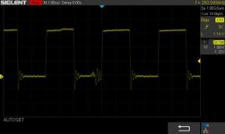
The frequency at A0 (6502 pin9) is 250Khz, is it correct?

SDS00001.jpg
 
Commodore PET ROM / RAM replacement board https://d3s5r33r268y59.cloudfront.net/datasheets/10158/2018-10-28-23-02-19/PET%20ROM%20RAM%20Board%20User%20Guide.pdf
This board has 9 DIP switches:
1-2 - RAM replacement options
3-5 - ROM replacement options
6-9 - ROM selection

used switches
1-2 ON (pcb Ram replaced by Ram board)
3- ON 4-5 OFF (pcb Roms replace by Roms board)
7- ON 6-8 OFF (BASIC 2)

In this scenario the pet uses the ram and roms of the replacement board....

I used this configuration to verify that the garbage error was not caused by the ram or roms.

With the NOP generator I am using the ram and roms of the pet.
 
That looks right. I thought the NOP would execute faster but it must be a two cycle instruction. Shows how much I know about the 6502.

You are doing good and will get to bottom of this problem.
-Dave

Yes, NOP takes two cycles (one fetch from memory, one idle cycle). A0 toggles each two cycles, so A0's edges happen at 500 KHz rate, but its actual frequency as a square wave is 250 KHz.

Frank
 
With a nop generator under the 6502, I'd first check each address going through UC3 and UB3:

Input and output from the buffers must be the same for all addresses. Since the garbage pattern is exactly 16 bytes wide, I'd pay special attention to A4 (AB4 on that schematic) and its path.
A4 path to the RAMs goes through UE5, that's the second place to look for problems:
Finally, should it be only a video RAM issue (I don't believe so however), there's UF5 that passes BA4 to them:

HTH
Frank IZ8DWF

6502 Output Khz (AB0 to AB7) are the same as the input and output UC3 (BA0 to BA7)
6502 Output Khz (AB8 to AB15) are the same as the input and output UB3 (BA8 to BA15)

BA4 output UC3 (15,63 Khz) is the same as the input pin4 UE5
BA4 output UC3 (15,63 Khz) is the same as the input pin13 UF5

What other pins and values must be checked in UE5 and UF5?
 
How many times do you bend the pins on a 40 year old part?
I vote for two sockets.
Dwight

Not sure what you mean; the relevant pins of the socket are bent out and up and connected appropriately (with a piece of paper underneath to prevent the bent out pins from touching the system socket), and the 6502 is just normally inserted into the socket.

But sure, if you have two sockets that works as well and no piece of paper needed.

If I could find mine I'd post a picture ;-)
 
Back
Top