• Please review our updated Terms and Rules here

Project to create an ATX 80286 mainboard based on the IBM 5170

I have been testing and saw some inconsistent exits by the CPU from RESET.
This lead me to believe that for some reason the clock pulse was not stable of not of sufficient level.
So what I did was to make an addition to the clock generation PCB where I added the 82284, but only to generate a clock signal, nothing else.
So basically I am using the 82284 as a clock generator only, no READY logic, no RESET control.
So inside the CPLD, nothing changed compared to my tests.

The clock pulse from the 82284 output appears to have cleared the inconsistencies of the exit from RESET.
So apparently the clock phases before were not of a consistent duration which leads to the CPU losing synchronization to the clock, which would be undesirable.
I also discovered another fact, the 82284 is able to run clocks of more than 40Mhz because it was oscillating at this frequency on the veroboard setup.
The reason is that the PCB has no traces so there is hardly any stray capacitance on this setup.
I even had to add some 10pF load capacitors in order to get a stable clock from the 82284 output.
This opens up the path to doing the 20Mhz tests again but this time with a normal crystal tied to the inputs of the 82284.
I just need to do this off the mainboard and it should work then. This will enable new tests for later at 18Mhz, 20Mhz, etc.

For now I will keep testing at the proven normal 32Mhz 286_CLK with the 82284 as a simple clock pulse generator, so I can focus my work on the 82284 and 82288 replacement logic, and I will revisit generating and testing the clock in other ways later if and when I have the 82284 and 82288 replacement done.

So, regarding the state and system control replacement logic, apparently the practical situation is different from the design. Which will almost certainly be a timing issue.
So it will be a hard process of many steps to get through, because I can't measure multiple signals, signals inside the CPLD which don't go outside, and I can't compare signals in real time with the cheap equipment I have.

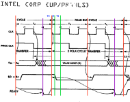
So, what I am doing now is to look at the timing diagram, and going down the process of comparing the theory with the actual situation to check if these signal states are reflected in the signal outputs of the logic. I will use the state machine as a reference where the CPU states are compared with the diagram.

I made a test output pin on the CPLD for which I borrowed the UART clock output.
So I am programming the CPLD each time to output something on this pin, and then measure it.

In that way, I am able to compare coinciding of signal outputs by using an AND gate to decode those signals together in the correct polarities inside the CPLD.
If I measure a response on the test pin, I can know if these signals coincide with each other.
This can allow me to verify sections of the whole logic, and try to trace the issues.

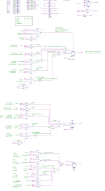
I changed the logic in the CPLD from the equations into positive logic notation equal to the PAL equations as much as possible, to reflect the actual situations that I need to look at.
Since the PAL article contains the state machine probably written in the same logic polarity as inside the PAL, regarding all pins as positive signals (I can't be sure because this is not mentioned), I want to see if in the CPLD the same things occur which are described in the article, and in the timing diagram published by AMD.

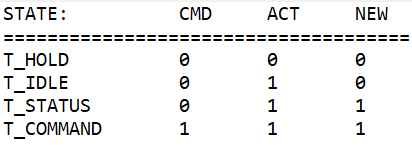
So I am now generating separate signals for the IDLE, TS2, TC1 and TC2 state.
And when these are reflected to need to be active in the decoders in some inputs, I substituted the logic in the decoder with the signal names of the T states.

This makes the logic a bit more "readable" for human eyes and it is starting to make more sense.
This does give me more confidence that the concept is sound, not that I doubt Dougs design, but I need references to check against.

So I am verifying sections of the CPU operation and AT functions step by step.
Since the 286 wants to load and execute the BIOS code, it is the first activity that should happen after getting out of RESET.
The 286 CPU is synced to the clock phase of 286_CLK by the logic inside the CPU which is connected with the point of exiting RESET.
That's why it's so very important to both enter and exit RESET at a precise moment during the falling edge of the 286_CLK, called the system clock by Intel.

I want to find out if the CPU is actually doing certain basic operations correctly, so I can have some idea about how viable the system would be with this solution.
Or how to get it into a viable operation of course.

Also I am trying to find out exactly in what area the cause for the missing READY pulses can be found.
The READY mechanism involves a lot of logic which needs to be traced through.
So I need to start at the memory read operation which would trigger everything else in the AT system control logic.

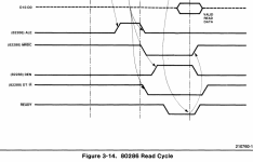
The first step is the T_TS2, the "send status" phase of the 286 CPU cycle.
The CPU exits from IDLE state, it wants to do a memory read operation and sets up the address lines for the correct address it wants, and at the same time it pulls S1 low. (memory instruction or data read).

This is detected by the state machine which decodes this and enters into the T_TS2 state at the next falling edge of 286_CLK.
The ALE signal is raised high and latched by the ALE decoders in the CPLD and this loads the address states of the memory location into the address latches.
So we should see T_TS2 entered while S1 is pulled low and ALE being raised high.
I was able to verify all these events happening simultaneously, so this is good news because the system is at least doing part of the operations correctly.
It would not surprise me if as soon as I solved the READY issue, the whole system may suddenly initialize as well.

So the address lines appear to be setup and latched.
Next step is the T_TC1 state.
I will do measurements on this next, and try to determine of this state is happening correctly.

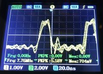
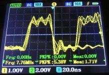
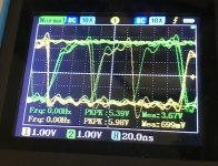
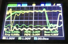
I attached a scope photo of the combined signals: T_TS2 & ALE & S1_n
The scope is of course of poor quality especially at this frequency, but it's possible to make out positive going pulses of roughly 50ns.
The 286_CLK period which covers the T_TS2 phase is 31.25ns so possibly the signals are high during the entire clock period of 286_CLK.
286_CLK clocks the state machine, so if this is active, we can assume the active period is exactly one entire clock length of 286_CLK.
After that the state machine will transition into the T_TC1 state.

I will update the test results as soon as I have more information.

Kind regards,

Rodney
 

Attachments

  • Img_4119s.jpg
    Img_4119s.jpg
    104.9 KB · Views: 2
Last edited:
I have completed more tests, where I found out that during T_TC1:

- both S1 and S0 are going high
- the MEMR signal is active

However, what should be happening is, ALE should go low during T_TC1 and T_TC2. This needs to happen so the address latches can keep the correct address line states, or else the information may be incorrect on the BIOS ROM adress lines. There is a problem apparently which causes ALE not to go low at all during T_TC1 contrary to the timing diagram in the AMD article.

The ALE signal is also part of the logic that clocks ARDY_n high, which initializes the PC/AT system control shifting circuits upon which the whole READY timing is based. The rising clock generated by ALE appears to be happening however since this signal is not correct, I will need to trace back exactly when it is active and when it is inactive. If the timing of ALE is incorrect, this will cause issues with cycle termination and the conversion process. I am going to trace ALE throughout the different states of the CPU to see where it is high and where low, so I can get a complete picture of the behaviour of ALE.

I attached a scope photo of T_TC1 combined with MEMR.
 

Attachments

  • Img_4125s.jpg
    Img_4125s.jpg
    105.2 KB · Views: 1
The ALE signal is definitely not working correctly.
The signal is active high during approximately 60ns periods which is double the time it should be active.
I checked the Intel 286 datasheet which also is showing ALE active high during only a single 286_CLK period.

So I will need to look into this and verify the logic to see why the ALE signal is not being clocked low during the transition from T_TS2 to T_TC1.

Below is the current, incorrect wave shape of the ALE signal.
 

Attachments

  • Img_4129s.jpg
    Img_4129s.jpg
    92.4 KB · Views: 4
I managed to fix the ALE signal to only be active during T_TS2 with some modifications to the ALE circuits. I now have an ALE signal which is active during what appears to be roughly the entire T_TS2 state. Basically the reason for the ALE signal staying active during T_TC1 was that the S1 and S0 signals were not raised fast enough by the CPU, so at the start of T_TC1 they were not fully established high. So in this situation, the logic for ALE failed to negate the signal. This makes me pause to consider that this may have secondary reasons, specifically that there may be a problem with the CPU clock signal still. I will keep this in mind during the continued debugging process. As I mentioned, in the future I really need to revisit clock generation and find better ways of generating a fully stable clock with proper edges. Right now, at least what my cheap scope is showing, is that the clock going into the CPU is sine wave shaped. And this is what is coming out of the 82284 which I am using as a clock generator only in this test setup. Probably I am better off finding a more modern clock generator chip which has a reasonable package shape that is possible to solder with a hobby setup and enough care. And of course I would need a chip which will be obtainable in the foreseeable future. Otherwise maybe I need to look into some FET circuit that is able to switch at very high frequencies. I don't need a super square wave, and we would not want that, however something slightly better than a sine wave would be desirable. Basically I want to see a very stable zero transition time so the timing is very dependable.

Now it's time to move on to other areas of operation in the AT system. I am seeing initial ARDY pulses being generated, so I need to check the source signals to see if they are all active. I will also verify DATA_CONV and END_CYC_n outputs to see if these show activity during T_TC2. If that is all verified, I will continue to check ARDYEN which serves to qualify the ARDY pulses. If that happens, I should be able to get the READY signal generated somehow with some modifications in the logic. Part of the READY logic also samples the S1 and S0 signals from the CPU though hopefully during T_TC2, they are already well established as both being in high logic state.

I am thinking, there is a chance that I am trying to fix something which is partially caused by a not so great clock signal. On the other hand, if I can get the signals stable under these conditions, this may also create a more robust timing when the clock becomes more accurate later on. I have seen that the system is very sensitive about the clock input. So decreasing this sensitivity may benefit the system to be operational at higher clock speeds.

I received some normal 40Mhz crystals of recent production, so I will be able to test these out soon as well. For now I want to explore these new state machine and command control circuits to get some experience working with these types of circuits in the AT system. The experience I am gaining now will benefit any situation later on and can inspire new ideas as well. Basically we now have a larger part of the AT system inside the CPLD which can provide the means to further integrate logic with eachother, which previously existed in different ICs and circuits. Even the quartus compilation process is likely to do part of this integration automatically already.

Kind regards,

Rodney
 
I have spent some time studying the AMD 82284 and 82288 replacement designs and I have done tests with a few modifications in the circuits. I tried to fix some timing issues which occurred in my setup using this design inside the system controller CPLD. This succeeded only partially, I managed to get a good ALE signal, and to sustain some READY operation for only a few seconds until the CPU crashed. Not enough to know if it could initialize or not.

Also I am not clear about the ARDYEN flipflop in the 5170 schematic because I don't know if this IC experiences the condition of being preset and cleared at the same time. So I replicated the TI design of the 74LS74 from the datasheet in order to create the situation where Q and /Q would both become high if clear and preset were simultaneously applied to the circuit. Since I don't know what's inside the CPLD D-flipflops, by using NANDs I could at least create that same design which does produce two high outputs.

It's my theory that in the system configuration of this project, the timing of the AMD solution is too far off to be able to run this cycle control and termination method reliably. The CPU timing is even faster than the other logic in the system controller CPLD, so it must be more critical to replicate those ICs. So I think this is pushing the limits with the speeds I want to use these circuits at. Also it looks like the CPU's own timing was somewhat off in my test setup to be able to operate those decoders reliably and with enough timing for the decoders to be able to function. Some logic is based on "same state", while other logic depends on having the signals for the next state ready on the inputs. Specifically the S1 and S0 signals seemed to be slow as I measured them, compared with what the timing diagrams show, and what the logic depends on to switch and store outputs on the falling edges of the CPU clock between the CPU states. Anyway I am sure the design is valid and would work for example if used with 5170 or similar system with a similar amount of TTL logic instead of using CPLDs. But for this system it seems not sufficient. I tested at 16Mhz and at 8Mhz CPU clock. Especially the decoding based on S1 and S0 seems to be off the most. When replacing it with alternatives, this did provide some improvements.

I had an idea to reverse the matter, I mean, to prepare the logic to generate all the control signals, and then in a working system, enable them one by one while disconnecting the from the 82284 and 82288 to the PCB to see if these signals in question are of sufficient timing. I could start with ALE and /MEMR for example, to see if these work. That way I could work my way up to a full replacement and identify where the timing is causing issues. However this is not possible because Doug Kern only published a reduced and modified state machine, not an identical method with the original Intel designs. With this published design, which is arguably faster running, I cannot be in sync with the UMC 82284 and 82288 chips because they operate on a 5 fold state machine. So it would be required to design a new state machine and decode based on that. I will look into this as well, however it seems that the state machine would then need to depend on 3 state bits, which would probably require more complicated decoders, with further delays and timing issues possibly being created.

Anyway, this design is really intriguing nonetheless and I'm grateful to AMD for at least publishing this because it can inspire new ideas. For example, using a really fast FPGA, there is a much bigger chance that the timing would be able to keep up with the CPU at a 32Mhz 286_CLK. The state machine transitions would be really fast beyond what I believe could cause issues. Also an FPGA compiler may speed up the logic of the state machine even further which could make for even better timing.

I will keep this design in mind, and I will experiment further when I am sufficiently experienced in programming and using FPGA's. Anyway, at that time I would possibly be better off to switch to a 486 based prototype because there would be much more speed increase possible to be gained.

I was able to get the UMC 82284-12 to oscillate at 40Mhz by directly soldering a 40Mhz crystal on pins 8 and 9, and separating pins 8 and 9 from the PCB using a socket with these pins missing in between, however this also resulted in a situation where the VGA didn't initialize properly and I got the same MR BIOS beeps as when previously using the external oscillator.

Whether this method of directly soldering a crystal onto the 82284 pins works depends on the properties of the crystal as well. I believe if the crystal is newer production, it is probably of higher quality and there is a bigger chance of getting it to oscillate on its fundamental frequency on a 82284. For example, a slightly older crystal of slightly over 36Mhz only oscillated at 6 or 7 Mhz CPU clock speed. If I can find a really new crystal of 34 or 35Mhz, I believe there is a chance of getting above 17Mhz which may still be able to operate correctly. If I find some such crystals, I will order them and test them out.

I will think about what I will work on next, I will search more information about state machines to see how these could be most efficiently created using normal logic or possibly some other methods. Also there is still some room for improvement in terms of clock generation so I will try to find more information about this subject as well. If I can generate a clock with somewhat better defined edges, this could possibly raise the maximum clock speed of the system. Possibly a much more modern programmable clock generator could provide an improvement for the system.

Kind regards,

Rodney
 
Last edited:
After my test experiences with the AMD PAL example by Doug Kern, I have become more interested in 286 CPU cycle control and decided to look into the Intel cycle model further.

I hope that recreating the original Intel model may enable me to experiment with partial functions being covered by the 82284 and 82288 while trying to take over others one by one with the System controller CPLD. The more control signals I am able to take over, the closer I will be to replacing the 82284 and 82288.

So in order to do this I will need to design a new state machine which runs in sync with the original Intel "double cycle per CPU state" model.

When studying the Intel datasheet timing diagrams I am seeing some difficulties which are not noticeable in the AMD timing diagram. However since I measured similar behaviour by the CPU before as seen in Intel's diagrams and diagrams of other support chip manufacturers, I am leaning more towards those being accurate.

In the Intel diagrams, the S1 and S0 status output pins of the 286 CPU are changed by the CPU asynchronous to the clock cycle period boundaries. That means that sampling them precisely at the clock boundaries will be useless to transition the cycle machine in some cases because at those times they will not reflect the changes yet which we are interested in.

In my attachment below I tried to illustrate this. At the state cycle boundaries(red lines) the changed state of S1 or S0 is not fully established, this occurs outside of the boundaries. So switching from T_IDLE to T_STATUS exactly at the cycle boundary will be impossible because there is no way I know of to decode before hand if the CPU intends to lower S1 or S0 a moment after the cycle boundary.

Depending on S1 and S0 for exact timing, looking at the timing diagrams, is not a good idea, so I need to choose different solutions for detecting these events.

Additionally, I had a closer look at the CPU state diagram as supplied by Intel, while evaluating this also looking at the 82284 pins, the 82288 pins and taking into consideration that we also have a T_HOLD state.

I want to design the state machine slightly different from the typical method. Normally this method would say we have 4 states so we need 2 state machine bits. But for my purpose I feel it would make much more sense to reflect the actual situation with three bits. This in the hope that later, perhaps less decoding logic may be needed. If that works out or not, I will keep this method for now unless there arises a need to change it.

So I decided to create a state machine using 3 bits. Below in my attachment you can see a table of the states and the three bits reflecting each state. The bits are called CMD, ACT, and NEW.

Since there is a need to make an asynchronous adaptation of the state machine, what I will try to do is to always transition from T_COMMAND to T_IDLE as soon as the wait state period is ended by READY being asserted low. Also exiting from CPU hold will always transition into T_IDLE.

The reason for this is that at T_IDLE, during the first quarter of the state period, between the green lines in my diagram, I will sample S1 and S0. If one of these goes to zero, which is the indication by the CPU that it intends to start a new cycle with T_STATUS, I will then immediately transition the state machine from T_IDLE to T_STATUS, asynchronous to the clock. So there will always very briefly exist a T_IDLE state in any case, until S1 and S0 are ready to be sampled which can enter the state machine into T_STATUS. If the CPU doesn't start a new cycle, the state machine remains in T_IDLE until the full state cycle has completed and another sampling of S1 and S0 can occur. The state bit NEW indicates the instance that the CPU has started a new cycle and exited T_IDLE. So switching to T_STATUS is slightly asynchronous, I don't see how else I could do this and I believe that it will not be of any importance, and possibly even done in some similar way by Intel. Unless I am missing something else.

The state bit CMD indicates that the CPU is transitioned from T_STATUS into T_COMMAND. This bit will remain active during wait state state cycle repeats until READY is sampled low so the state machine can return to T_IDLE, where S1 and S0 are sampled again.

The state bit ACT specifically can indicate if the CPU is active, or in T_HOLD. This is controlled by sampling CPU_HLDA during T_IDLE which would tri-state the command outputs and then further transitions into T_HOLD at the next state cycle boundary. T_HOLD is maintained until CPU_HOLDA is asserted low, which at the state cycle transition will always cause the CPU to enter T_IDLE either briefly or for an entire state cycle period.

So that's my concept for now. I am not sure if it reflects Intel's method, however I hope that it may be accurate enough to be able to predict in next design steps where which control signal needs to be activated.

I will look into designing all the state transition logic next. As soon as I have a concept of this, I will share the schematic here.

So there are three design steps ahead:
- functional design of the state machine
- design the command decoding
- design the command and control output logic

Kind regards,

Rodney
 

Attachments

  • STATES_AND_BITS.png
    STATES_AND_BITS.png
    3.8 KB · Views: 3
  • S0_S1_ASYNCHRONOUS.png
    S0_S1_ASYNCHRONOUS.png
    66.1 KB · Views: 3
Last edited:
I have finished the logic for transitioning the state machine, at least this is what I have come up with, and remains to be tested further in the System controller CPLD.

In the attachment I tried to get a bitmap from quartus which is a little buggy but visible.
This is my rough draft which contains my notes which I used in order to get an overview on whether the whole circuit is complete and covers everything.
There are some duplicate circuits but this is not relevant to look at since quartus compiles all the circuits anyway and will reduce the logic automatically into the most reduced equivalent, which is what we want.

So I got all the CPU state transitions decoded as far as I can determine at this time.
I still need to interface it with the rest of the core AT logic, one thing I will need to do is to decode READY so the cycle termination will work correctly.
Also I will need some connection with the HOLD mechanism of the CPU in order to decode this state transition correctly.

After I have these things sorted out, I will do some first tests by trying to generate the ALE signal on a test output.
I will use my cheap scope to compare the test output with the ALE generated by the 82288.
If I can get the identical signal created, I can do some first functional tests by replacing ALE with the new logic output and disconnecting the ALE pin from the 82288.

ALE needs to be generated exactly right, because this signal is used to clock the wait states for the cycle termination decoder.
The wait states are clocked through the shifter and then control the END_CYC_n logic which controls READY.

So I will first work on integrating the state machine into the System controller CPLD.
Then I will add the new ALE decoding circuits and compare the output with the 82284 ALE output.

Hopefully I can get this state machine based system to work identically to what Intel designed in their chips.

Kind regards,

Rodney
 

Attachments

  • 286_AT_CPU_state_command_controller.png
    286_AT_CPU_state_command_controller.png
    69.4 KB · Views: 5
Hey Rodney,

Happy to see you are continuing with some progress. 8088s get a lot of attention and 286s are generally ignored so I'm glad you are trying to build a pretty good 286, and not just some 6-8 mhz system. The hardware design here is way beyond my hardware knowledge as i'm mostly a software guy and a tinkerer/overclocker - but I'm glad you are documenting everything you are working on. Maybe after I study hardware some more, it will make some more sense to me.

I read through some things and noticed the SRAM is on an isa card with the memory controller essentially being a CPLD, is that correct? Is that working with 0 waitstates? if so that's really cool. I didn't realize the CPLDs were reprogrammable at all, I think a lot of the 16 bit XMS/EMS memory cards use them.

The Harris 20-25 mhz chips are not too hard to find. Some still exist new old stock (either harris or intersil) usually around $10-20 USD per chip. Mystery used chips from China are around $4-5 USD per chip in bulk, and depending on the seller the counterfeit rate is around 5% or 100%, but they will usually refund you anyway. It's very easy to tell the counterfeits - they have no text stamped on the underside. Funnily enough, I purchased 25 NOS intersil/renesas chips and they all ran pretty much 25-27 mhz max, but those used chinese harris chips do like 24-34 mhz. The average chip does seem to run stable 15-20% over its labeled speed, though, whether its a 16 or 20 or 25 mhz part.. I have probably purchased around 75-100 of them by now, binning them for overclocking purposes (I've run them up to around 37 mhz before). Anyway, if you want a couple good reliable chips I will happily mail them to you.

Aside from Wolf3D, another pretty good benchmark is 3dbench. I believe this is the link to it: https://archive.org/details/msdos_shareware_fb_3DBENCH.
 
Hi sqpat,

Thanks for your reply, I appreciate reading your message. And thanks for taking the time to read more about the project, I realize it's a lot of information, the project and resulting system is complex and there is a lot of work involved to get it to move forward even further. Everything is documented and shared in full detail on my GitHub.

Recently I made some updates to the GitHub and I have uploaded the extensively tested 16Mhz quartus projects and CPLD JED files needed to build the system in a single archive, those are what I am testing with currently. I am using "Quartus II 13.0sp1 (64 bit)" to create the designs and prepare the POF files, which are then converted with POF2JED into JED files and programmed into the CPLDs. The JED files are in the archive so "all" that is needed is to program the CPLDs with these. If at any time later you decide to dive deeper into the technology, I would be happy to elaborate on any unclear areas. Getting a full understanding of the AT is really a great thing, and helps us to appreciate the design by IBM even more. I mean, in the 90s we were using these systems, but now the matter is purely from the appreciation perspective for me. I just love using this test system, it's super responsive really. I even played Doom8088 on it several times, a really great project too, thanks to the amazing work Frenkels is doing on that project!

Right now I am focusing on moving the 82284 and 82288 completely inside the CPLDs. I am hoping to accomplish that this can raise the clock speed and even higher stability at above 16Mhz. When I have the system control and CPU state control fully integrated into the System controller, this can enable tweaking the system even further in the future. Basically this work is the extension to complete the Intel 286 concept for a full system. The CPU as described in the Intel datasheet is only part of the design, and the state and command control logic is also needed to allow the 286 CPU to work as described in the datasheet.

I am not sure yet if CPLD technology is fast enough for this purpose, I may need to find other solutions like an even faster FPGA. It's a process I need to go through in order to get more experience in this area. If I do design a follow up mainboard, I will put the CPU on a module PCB so it will be more easy to swap for a 486 or FPGA core. And I will try to use even higher integration with larger pin count packages so there will be more board space available for integrating the memory subsystem on the mainboard.

That's right, I moved the RAM together with the memory decoder on a ISA card to plug into an ISA slot connector. The card has a custom 10 pin connector which can be connected to the mainboard using a standard 10p flatcable with typical press-on flatcable header connectors. The full 286 memory map is decoded on the ISA card so theoretically it could supply 15Mb of RAM to the system. The 16th MB is sort of "reserved" for ISA slot cards. Anyway for most applications of a 286, 4 or 8MB is more than enough I think, I just added the rest because there was space on the card anyway. The memory decoder is running a default configuration right now since this is the prototype and my initial goal was to get the system functional. So the 16 bit RAM access is done with one wait state, in the future I could wire up the 0WS ISA pin to the CPLD and control this line during the RAM access decodes to reduce that to 0 wait states. When I test this later, I will post the test results here.

There are some "one time programmable" CPLD types like the EP1810LC and others. Those might be used by some manufacturers in the 90s. The ATF1508AS CPLDs I am using can be reprogrammed at will. I reprogrammed the System controller over 200 times during my tests, and this was a used recycled chip. I bought 10 CPLDs total of which 6 were programmed not to have any JTAG inputs anymore. So those are useless basically. The other 4 are three 10ns types and one 15ns chip.

I have looked at the Harris and later Intersil CPUs on Ebay, the problem as you also mentioned is getting a CPU which is original. Your tests at above 30Mhz must have been able thanks to having real CPUs which were not faked. I will PM you my address, if you have the time to send me a Harris CPU which you have confirmed to work above 30Mhz, I would appreciate that because at least I can then be sure it's a "real" CPU. I could use that 25Mhz specified CPU which you have confirmed to work at above 30Mhz as my new main test CPU for my future test work on the system. If you have the chance and time, that could be useful for the project.

Thanks for pointing out 3DBench, I have tested it on the system at 16Mhz and the score is 4.5 fps.
I recently also tested with VIDSPEED.EXE and the test results are also in the attachment. I only tested as many modes as can fit on a screen photo.
Theoretically if I set 0 wait states for the SRAM, the first test should result in higher score because I think this program is just testing the normal RAM throughput with the "*" test.

Great talking with you sqpat,

Kind regards,

Rodney
 

Attachments

  • Img_4269s.jpg
    Img_4269s.jpg
    183.1 KB · Views: 3
  • Img_4265s.jpg
    Img_4265s.jpg
    126.5 KB · Views: 3
I have made some substantial progress. After some tweaks to the state machine logic and the logic which connects it with the other System controller logic, it now looks like the state machine is accurately following the CPU state activities according to the Intel state model.

So I proceeded to work on the ALE signal. During this work it has become apparent that these recent updates are really testing the limits of the CPLDs used. The specified speed of the CPLDs is 10ns. And I am working with clocks of 31.25 nanoseconds. Certain logic which is theoretically sound is apparently not being triggered at these speeds.

I finally managed to create a circuit to generate ALE using the T_STATUS condition of the state machine. Using the dual channel cheap portable LCD scope I could see that the ALE test signal generated by the CPLD was nicely following the original one coming from the 82288. So I proceeded to put a socket between the 82288 where I removed pin 5 and changed the ALE input to an output on the CPLD. Then I connected the new circuit to the ALE net in the CPLD and updated the System controller. After the update I saw the PC come alive right away and it produced the POST screens, however during boot time the PC froze. So it appears something was not 100% in sync(yet) and during boot time this becomes apparent. I tested by going into MR BIOS and I was able to control the BIOS and go through the menus fine without any freezing while leaving the PC in the BIOS screens.

So as a test I decided to change the logic to decode from S0 and S1 directly from the CPU. This event to generate ALE is during the second clock phase anyway so S0 and S1 will be well established by then. This worked even better and I was able to fully boot the PC using the new ALE signal, and I have run a Wolf3D demo for about an hour without any issues.

I will do some further modifications to try to improve the accuracy of the state machine control of ALE, possibly I can still get it to work using the state machine timing. I am thinking to sync the different command states another time and just using a state signal which is active when a particular state is active. Possibly this can produce even more precise timing and could keep the ALE signal running properly controlled by the state machine.

After I am done with ALE I will continue with other control signals in order to attempt to replace those. A next candidate is the DEN signal which is internally decoded by the CPLD. This could possibly free up an extra CPLD pin which I could use for other purposes later.

Kind regards,

Rodney
 
I have tested some more and I was finally able to get ALE working after all on the new state machine, which is great and the first solid application in the system for the state machine logic. I am now running a short demo of Wolf3D just to check stability. I have booted from floppy, tested with VIDSPEED and did some tests with checkit. They all seem to pass fine with the new ALE signal on the state machine.

I have done the first tests to generate the DEN signal which is only used to control the databus transceiver decoders, nothing else in the system. So the signal wouldn't need to go outside the CPLD.

I am able to match the start timing it seems however the duration is too short, so something needs to be fixed in the decoders.
I have tested and was able to get a POST and VGA display is initialized with the new signal but it's not entirely right, which I can also see on the scope in the durations.

One positive thing about the CPLD supplying DEN, the amplitudes are much higher than the 82288 DEN output, which may possibly benefit testing with higher clock speeds in the future. Also the integration of these signals could hopefully improve the timing as well. Though there is still the concern if the CPLD can be fast enough.

I will test further and work more on the DEN generation logic.

Kind regards,

Rodney
 
The specified speed of the CPLDs is 10ns. And I am working with clocks of 31.25 nanoseconds. Certain logic which is theoretically sound is apparently not being triggered at these speeds.
There is a suspicion I have about doing CPLD logic with Quartus. Maybe somebody here knows for certain. If you have two registers with the same clock input, and you want both of them to latch a new value at the same time, but the new value of B depends on the old value of A, it doesn't work reliably (but also does not produce a compilation error). This does work in an FPGA. Maybe Quartus does adequate management of setup/hold times for FPGA targets to guarantee something like that, but not for the older CPLDs?
 
If you have two registers with the same clock input, and you want both of them to latch a new value at the same time, but the new value of B depends on the old value of A, it doesn't work reliably (but also does not produce a compilation error).

Hi bakemono,

Thanks for your reply. I am also wondering about the timing details in such cases. I try to reason this matter in terms of "N" and "N+1", so the evaluation is reasoned to take place within the clock period, and will become apparent in the next. I think quartus also assumes this as the desired result. It seems to work properly in most cases however I did eventually have some problems with derived signals from the state machine. If I push it "too far", the logic won't be able to cooperate, and during the design you already start to get some expectation, but not for certain, that this may possibly come into play, just like you mentioned.

For example, I tried to combine the state bit outputs into a single signal to signify that particular state being active, and use that signal as a source to clock another signal, however I found that the timing could not be reached to allow the state signal to transition at the same clock and update that signal "in time". So what I did in that case was to use all the state machine bits in an AND gate instead as an input to control the clocked output signal. And there, a clear difference could be observed where in one case I had a PC design which froze, and in the other case I had a system which worked completely stable. A clear test example where you can actually see differences in operation. So when combining clocked signals at the same transition and trying to clock that result another time was not fast enough in this case to be "caught" on another flip flop. So I switched back to a circuit with combined signals in an AND gate with 6 inputs, which worked substantially better.

I also found that after changing the clock pulse of the state machine to be more defined, this made the switch timing of the output signals much more precise and earlier. I could see the change of a few ns earlier even on my cheap scope because I was comparing the signal from the CPLD to the original one from the 82288. So using a better defined clock signal also improves this matter of switching speeds a lot.

Quartus is really great software and I came to appreciate a lot of smart things in the software, though the risk is there that it may also automatically assume something which throws off the timing. At the start of the project I had a lot of trouble with this fact and needed to make modifications to solve it. If I understand it correctly, quartus tries to eliminate shift registers if it believes they can be replaced with fewer elements. However this is much more sensitive to most exact timing to predict at which delay a signal should be asserted. So it is important to always enter the clock periods in the SDC file for the timing analysis. Defining a signal as a clock source can much improve the timing of the compiled result because it will be treated differently. Recently I also found and tested a compile option to turn off shift register replacement so I applied this option to get a more exact function of the logic in the wait state control. As a consequence I also noticed that the timing "errors" in the compile log became a lot shorter, like they were reduced to only propagation time values instead of like 20 or 30ns reported. Also, in case of CPLDs, if the chip starts to get really full in percentage, the compiler may do some undesired things in order to get a "fit". So getting a CPLD really full is not a good idea for any design. Thankfully up to now I have had ample space and no concerns in that department.

Anyway, I really want to make the transition as some time to using FPGAs simply because of wanting larger pin count devices, and also because of needing faster speed to be able to do more in terms of transitioning multiple signals at the same exact clock time. Sometimes signals are on different clocks which do transition at the same time so it's the same problem as you mentioned. I think using flip flops is the best circuit approach because I believe these are also handled differently by the compiler. So this may have advantages which are not immediately visible to the designer, however apparent in the test results.

It can provide insight to look at the "technology map" which quartus generates and on which the fuse map will be more closely based, however since we are not computers, this will take up a lot of time to select signals and see in the map where they came from and end up. Quartus does at least provide a good highlight of the net when you click one, so you can trace it where it is connected in other areas. But it can consume a lot of time to understand the technology map results, and it definitely is not a schematic. If they provided signal names in the diagram, that would have been much easier and faster to "read" the technology map. In order to do that, I suppose it could be printed and processed. Another disadvantage is that quartus makes its own "elements" from the instances which are kind of "black boxes" because they all look the same in the diagram. So it's much less "human readable" than a normal schematic.

Kind regards,

Rodney
 
I am currently working on the DEN signal which enables the data transfers into and out of the CPU.

When studying the 82288 datasheet I am seeing rather elaborate mechanisms on DEN.
They look at the current and next cycle to decide the timing of when DEN will turn on and off. When transferring data into the CPU, the data transceivers need to be reversed, and they claim that in order to do this, the DEN signal would need to wait for the DT/R signal to reverse first before switching on the transceiver. And before the DT/R is reversed again for writing, DEN should be disabled earlier. Frankly, I never have seen this before, and I wonder if this is really needed. I have printed out the timing diagrams for the different scenarios which is great that they supplied these, and I could design something which stores the current cycle to be read or write, and looks ahead at the next cycle, and base the DEN timing on these two things, but I first want to test DEN in a normal and direct configuration without shifting the timing. What I want to do is to enable DEN during the entire command cycle. And I want to change the DT/R signal at the same moments, between the state cycles. If this kills a transceiver, which I doubt, I will see it happen and then I also have some certainty that it is really required. I will test the direct configuration first. If that causes some problems I will create DEN in the way they described. I am thinking, if I create DEN for the full T_COMMAND cycles, I also at the same time will need to create and replace DT/R for these to match during data transfers.

I will need to experiment a little with these control signals to see if it could work properly to use equal read and write lengths. When looking at the AMD timing diagram, this is also what Doug assumed. I think having a longer DEN signal available may enable to use less wait states in the system because during the normal T_COMMAND cycle we have sufficiently long enabling of the data to do the data transfers. These things are a little up to the discretion of the designer and can be tested to see if that would be viable.

Thanks to the Intel CPU cycle model, these control signals leave some room for experimentation, and at least in the datasheet timing diagrams I can make out when theoretically the CPU should have the correct data available, which would be longer than the actual T_COMMAND durations. I could experiment with standard longer enable periods for DEN and DT/R to have a better chance for the system to work at even higher clock speeds than 16Mhz. But first I will do some testing with a straight forward operation timing of DEN and DT/R.

Kind regards,

Rodney
 
I have done some more testing and experimentation with different types of circuits to see which ones are working the best in the System controller CPLD. I created the DEN signal only during the T_COMMAND states with various circuits, and I was indeed able to at least POST the system to a certain degree where the BIOS was showing messages, however soon the system froze so it was not completely functional yet with the new DEN signal to be able to boot.

When looking at the scope I can see that mostly the DEN signal seems to last much longer than single CPU cycles typically do. So possibly the DEN signal should be generated in the same way as described in the datasheets in order to get the system 100% functional.

This will require to keep track of previous cycles being read or write operations, comparing these with the present and coming cycles and to attempt to modify the DEN activity accordingly, for example that the write operations, if these are back to back, should keep the DEN signal enabled constantly throughout these writes, and when reads occur, to shorten the DEN duration considerably to be less than a processor clock even. The timing of this will need to be extremely accurate and I will try to find a way to evaluate the past and coming cycle types each time during the T_STATUS which then needs to modify the DEN durations.

I will first go by what the datasheets and the 286 hardware manual is showing in the diagrams, to see if I can replicate a 100% identical behavior to the diagrams. Possibly after getting the DEN signal to stay on across multiple cycles this will already give a big improvement in functionality. I just need to create circuits which are able to do this at the current clock speed.

I will print out the diagrams and work on the problem to determine circuits which can decide the DEN conditions at certain precise moments during the CPU activity.
Also I will study the manuals and read the descriptions by Intel a few times to get some ideas how to do this.

Kind regards,

Rodney
 
Today I made a complete new start on the DEN circuits. I have done a lot of reading in the Intel documentation.

This time I decided to discard the AMD method and only to attempt to follow the Intel timing diagrams.
I made circuits to latch the previous cycle type to be either a read or write type with two latches.
Upon a ready event the read and write type bits are clocked into a second set of latches to latch the previous cycle being read or write.

I separated the DEN control into start events and stop events.

Basically during a read cycle, DEN starts later and stops sooner.
DEN then starts after DT_R going low at the next 286_CLK rising edge, and is cleared immediately at the termination of the read command cycle.
The signal order seems to be according to the diagrams: DT_R low -> DEN -> COMMAND -> DEN OFF -> COMMAND OFF -> DT_R back high.
What I don't know in this case is if during back to back read cycles whether DEN and DT_R stay in their current state or return to inactive as seen in a single read cycle diagram.
I couldn't find any diagrams of this condition of repeated read cycles back to back.
I assume they are not staying active because it's impossible to know the next CPU cycle whether it is read, or write, immediately after T_COMMAND ends right on the state boundary.
The CPU takes a moment to assert S1 or S0 low if it intends to do a read or write.

During a write cycle, DEN is enabled much earlier, right after when ALE goes high during the second half of T_STATUS, and it persists throughout T_COMMAND until halfway into T_IDLE, or halfway into the next T_STATUS, unless the new cycle is also a write cycle, which then doesn't clear DEN and should keep DEN enabled.

During wait states, DEN is not cleared at all since wait states are also command states and DEN is not cleared during any command state either.

I printed out the timing diagrams and made some markings to try to determine how Intel created the control of DEN in the 82288.

I made some progress where my current circuits are able to initialize the VGA BIOS, do a partial POST and show the "Battery Backed Memory (CMOS) is Corrupt" message after a few resets. The keyboard controller is also initialized and I can see the numlock light on. The speaker does beep at the CMOS error so the timer chip also works.
However then the system freezes. Also the system is not detecting all the RAM so there is something not working right, probably related to the A20 logic control by the keyboard controller as well.

I will look in more detail at the state machine which controls the CPU cycles, and attempt to find alternative circuits to enable DEN during write cycles.
I am creating a READY signal in the System controller CPLD for terminating the cycles in the state machine, but possibly this method needs some modifications.

I have also thought about creating some kind of state machine to operate DEN, however the problem remains to find conditions to change the machine states.
It's not much different from what I am doing right now. Changing the approach seems to have improved things.
Also, DEN is irregular and changes state not at a single clock event. Which makes it harder to create a state machine for it.

I am also thinking that probably I should look into FPGAs and using VHDL or Verilog to describe the CPU states possibly in a more straightforward way.
I am not sure if the ATF1508AS 10ns CPLD is even fast enough to use certain circuits to set or reset DEN as fast as is required by the CPU at 16 Mhz.
The CPLD may operate certain logic however the question remains if this happens fast enough.

I am now able to get a partial post after some resets, so the system is running to a certain degree until it freezes.
Beeps happening suggest that conversion also must be working to some degree since the timer and keyboard controller operate on the 8 bit databus for example.

Kind regards,

Rodney
 

Attachments

  • Img_4365s.jpg
    Img_4365s.jpg
    109.1 KB · Views: 6
I have worked on the DEN signal a lot. Just for reference I am taking some measurements of the 82288 in operation, so the actual verified stable signals.

The first issue I am curious about is the timing of DEN relative to DT_/R during read operations.

So I measured on channel 1 the DT_R signal(yellow) triggered on the falling edge, and on channel 2 the DEN signal(green), both coming from the 82288.
This is a UMC 12 Mhz 82288, so a somewhat newer IC.

The first thing I am noticing is that the timing of DT_R and DEN during a read cycle are virtually identical.
So to create some elaborate system for controlling DEN during reads seems unnecessary.
Also in the example I am seeing a duration of 200ns which is most likely due to wait states happening.
I will check this in another measurement.

There are three conditions where DEN needs to be enabled for the CPU to do the operations:
- write transfers
- read transfers
- reads from the interrupt controller to get the vector data

So far I have focused more on the reads and writes, but I will look in more detail at the interrupt acknowledge timing as well.
I need to find a more precise timing diagram.

My cheap LCD scope seems not entirely up to the task, because I am seeing several instances of the same signal in the screen area.
Somehow there is one signal more clearly defined, so I try to ignore the "background".
At least I can see something and this can provide valuable information which I otherwise would not have.

The CPU documentation diagrams are elaborate, but I am getting the impression that the real situation is slightly different.
Just like with the solution from Doug Kern, he found a whole different approach which according to his article is supposed to work.

I am getting the impression that I may be better off to attempt to study the actual signals to see the timing from the stable situation.
Maybe the cautious approach by Intel was done because they were not sure of the failure reasons of data bus transceivers.
I think those will be more related to serious contention on the data signals. For example during memory reads if the RAM chips conflict with the transceiver.
However if the timing of DEN and DT/R is identical, there is no contention happening.
I have never experienced such a system failure where the transceiver died, except when I was taking some risks trying to erase some CPLDs from Ebay.
The CPLD surely caused a contention which killed the data transceivers, which is to be expected.

In the attachment is the scope photo of DT_/R and DEN as mentioned.

I will think of more measurements and try to assemble the DEN signal from the scope as far as this is possible.
Hopefully this can provide more insight how to adapt the logic circuits to generate DEN.

There is an additional modification to the operation of DEN in the AT, which I found in the 5162. There they added ARDYEN_n in the DEN circuits which enable the databus transceivers.

If ARDYEN_n is high(inactive), in this version of the logic this also enables DEN during additional periods on top of what the 82288 provides. Probably they did this to extend the periods of DEN and have a better chance of successful transfer operations. I have tested this modification for a few weeks in the prototype and this is indeed fully functional without problems. Since it's a modification by IBM in a later model AT system, and it works in the prototype as well, this could provide some improvements to the reliability of the system.
I will also try to do measurements of this combined signal to see what this looks like.

Kind regards,

Rodney
 

Attachments

  • DT_R and DEN Intel diagram.png
    DT_R and DEN Intel diagram.png
    45.5 KB · Views: 3
  • DT_R(YEL) relative to DEN(GRN).jpg
    DT_R(YEL) relative to DEN(GRN).jpg
    37.4 KB · Views: 3
Last edited:
After looking at the scope more it looks like DEN does follow slightly after DT_/R goes low, I think logic propagation could replicate this with asynchronous control of DEN during reads.

I checked the DT_/R signal against READY and indeed confirmed it's wait states extending DEN during reads. At the end, READY can be seen going low.
DT_/R is then returned high as well.

Kind regards,

Rodney
 

Attachments

  • Img_4371s.jpg
    Img_4371s.jpg
    135.8 KB · Views: 1
My thanks to sqpat, he sent me two CPUs which he has verified, one Harris which he clocked up to 32.5 Mhz and an Intersil which he got up to 28Mhz, pretty amazing speeds! The fact that he has verified those CPUs makes me 100% sure that these CPUs are not fakes, which is very useful in my work to have this certainty that at least the CPU should be able to run at high speed. I am currently using his Harris CPU in all my tests, rated at 20Mhz, but which can go up to 32.5 Mhz.

I have found a few issues in my state machine which follows the CPU operation states. Somehow the T_COMMAND state is not entered and exited.
So the machine only goes between the other states, which is not a complete function yet.
I need to fix the issue in the state machine and verify it with some signals for reference to make sure it follows the CPU correctly during all the states.
Later I will be testing the T_COMMAND state against the wait states I observed before when monitoring DEN during the memory read cycles.

Another issue I am having is that the ready timing is not entirely right. The READY signal is too early so I will need to clock and shift the ARDY_n signal to more closely match the READY signal coming from the 82284. I am trying to find a complete and correct description of the READY operation. When READY is working right internally in the CPLD, this also will help the CPU cycle state machine to operate correctly since this is also based on READY being a part of the cycles, to predict the wait cycles, exiting from T_COMMAND, etc.

The timing inside the 82284 is weird, they shifted the PCLOCK by 2/3 of the CPU_CLK. This appears to be synchronized to the timing of the CPU controlling S0 and S1 at the start of a transfer cycle. So I think there must be some programmed delay on the 286_CLK internally to achieve this time shifted PCLOCK. The timing is strange because it's 2/3 off compared to the 286_CLK, which is a weird amount. This timing is not so useful for other purposes, and not used for anything in the IBM AT design.

I will keep at it to try to assemble a complete "bus control" replacement so I can eventually remove the 82288 and 82284 from the mainboard.

I am thinking to at some point insert a FPGA into the system, and try to let the FPGA take over some functions.
My idea is to let the FPGA generate the clock to the CPU for example, this can make testing the system much more flexible.
And I am hoping that the quality of the clock will be higher so I can get a better synchronization of the CPU to the clock.

Eventually I want to test with a FPGA memory subsystem and perhaps even provide the ROM data from an FPGA in some faster way.
If I can replace a lot of logic with an FPGA this could reduce board space a lot, and provide faster speeds in the system.
So this way I hope to be able to reach zero wait states without any issues if the DRAM controlled by the FPGA can keep up.

I have studied some FPGA types which are 3.3V compatible like the Cyclone II, which is even able to interface with 5V systems using some resistors to limit the current into the "PCI clamp diodes" which are enabled with 3.3V operation. I saw some affordable small PCBs with 128 pins on the headers for example.

I also have a Spartan-3 starter board with 3 40pin headers, I will look into how I can possibly put this to good use for the project. This one is by Xilinx so I will need to look at what tools are available. This board does have some RAM included.

For now I will keep working with the CPLD because it's already in the system, and try to expand the functionality by replacing the 82284 and 82288 control.

Kind regards,

Rodney
 
I have studied some FPGA types which are 3.3V compatible like the Cyclone II, which is even able to interface with 5V systems using some resistors to limit the current into the "PCI clamp diodes" which are enabled with 3.3V operation.
"Officially" this is not guaranteed to work. The PCI clamp diodes are intended to control overshoot on 3.3V buses. Connecting 5V to it exceeds the maximum rating in the datasheet.
 
Back
Top