• Please review our updated Terms and Rules here

Project to create an ATX 80286 mainboard based on the IBM 5170

I took a 40Mhz normal crystal from a VGA card to test if the 12Mhz UM82C284-12 could oscillate at this frequency, however this didn't work.
The resulting internal clock pulse of the CPU went down to one third of what it should be, 6,66 Mhz.
This may be related to the crystal, or the frequency simply being too high for this type of oscillator circuit as well. I will try other crystals as well as soon as I receive some more. The problem is that when the frequency is raised, the value needed for load capacitance on the crystal drops below the PCB stray capacitance. So we need something like negative capacitance in a circuit, which may possibly involve a coil or needs an additional amplifier which would then start to look more like the crystal oscillator chip solution again. The other issue is that my cheap oscilloscope is not able to show any useful information about 40Mhz clock pulses for me to be able to really see the clock pulse wave shape quality. At the higher speeds, either all clocks look the same, or when looking in detail, I get a lot of distortion. So I am left with only being able to test different things and then observing the resulting system.

I read a lot of generic documentation about clock generators which show all sorts of circuits however it's not very useful information in a practical sense for applying in this project. I did see some coil information with really tiny values like in the pH range. Maybe by using some circuits which use a series coil, I could be able to get the crystal inputs themselves to oscillate with a normal 40Mhz crystal, so not by using a oscillator IC. Or if I can find a 40Mhz crystal which has much better specifications it may also work with the 4pF PCB stray capacitance loading it. I have thought about disconnecting the 82284 crystal pins from the PCB and soldering the crystal pins directly to the chip, which is a bit crazy but I may try it later. I mean, if it works, that would be at least something to test with.

How the clock is generated in the 82284 is a really sensitive thing at much higher clock speeds like 20Mhz, so results may vary depending on how it is done, and I will try different methods to see how they compare. I have ordered a range of normal "fundamental mode" crystals from different suppliers. Anyway, when I use a crystal oscillator chip on the X2 input, I do need to load the 82284 crystal pins with some larger capacitors like 18pf to have any chance of a POST. I hope I can improve this situation by trying alternative means of getting the 82284 to oscillate normally with a crystal using its internal oscillator circuits.

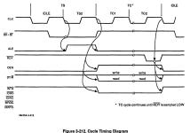
I am trying to compile a lot of information about the 82284 chip from various documentation and timing diagrams, and attempting to translate everything into actual circuits in order to assemble a equivalent schematic of the 82284. This is kind of tricky work because there is a lot of synchronization and delaying etc going on inside the chip, and not all situations are treated equal so this needs some additional circuits to evaluate the CPU cycle state condition. Also testing this is kind of dangerous and can seriously fry a system if there is an error. At the very least this will destroy the transceivers involved, if not more, which we don't want to happen. So I will need to do a lot of testing by comparison with the outputs with an actual 82284 to see if I am getting anywhere close enough to attempt testing it in the AT system.

Using the 82284 equivalent logic combined with additional decoding can subsequently also be used to control a 386 CPU in a 286 AT system, and most likely this also applies to the 486 CPU. The status and control output pins of the 386 and 486 can be translated back to generate the equivalent signals of the 286. This is also mentioned in some VLSI datasheets where they provide some PAL equations for this. Basically I think it also can be done by simply looking at what the status pins represent and translating this, though there may be some timing issues as well. I will also analyze the VLSI PAL data further if I decide to look at a 486 system, it may provide some further clues about what they found in their test work. For the final circuit of a 486 recreation I would probably use a combination of translating the status pins into 286 compatible outputs and using the 82284/82288 equivalent circuits, starting with a 486SLC type system which is close to the 16 bit 386SX. When everything is translated into normal circuits, possibly the logic can be reduced somewhat. So when we try to recreate a 486 system, it will be required to deeply analyze the CPU timing in full and complete detail until everything is completely known. The advantage is however that this knowledge may help to even further tweak the timing and may yield even higher processing speeds.

When I have been able to piece something together worth testing as an initial 82284 replacement, I will program it into a ATF1508AS CPLD and test it out to see if it could be functional. Replacing the 82284 will definitely help to improve the timing at 20Mhz and beyond when we can change the logic and use the much faster CPLD chip. Of course, I will share all the circuits and ideas here as soon as I have something functional resulting from my tests.

Kind regards,

Rodney
 
Last edited:
Since I like the generic 286 MR BIOS the most, I have tested more today and found a way around the COM port detection problems in MR BIOS.

What happens is that when MR BIOS doesn't detect the COM port, a few power cycles without the UART present, and then with the UART present can trigger a new detection which you can then save into the CMOS settings.

What I did this time is after a good detection happened and was saved into CMOS, I used a CMOS settings backup tool to save the CMOS to a file. I added two options in my config.sys menu to quickly be able to backup to a file on the harddisk and restore the CMOS from the backup.

Next what can happen is that when you enter the MR BIOS menu with CTRL-ALT-ESC or pressing escape during the POST, and then power down the PC, for example, next time when you power back on, the MR BIOS may report the COM port to be "removed".

Now how I can fix this is to choose to restore the CMOS from the backup from the config.sys menu option, and then just press CTRL-ALT-DEL, and at the next boot of DOS, the COM port has returned fully functional since it is again present in the CMOS.

This method works very fast and is the easiest workaround I know of in order to return the COM port function, without needing to remove the UART and putting it back in after a few power cycles. So restoring the CMOS is a quick way to fix the problem without needing to open the PC case, which is a big improvement. It's not ideal or perfect, but since I don't have any source code to review, I can't really know how MR BIOS is doing the detection, or losing it.

As I mentioned earlier, I have done quite elaborate experiments and modifications in the System controller and IO Decoder CPLDs however all of these never got rid of the detection issue. The UART has caused more issues in the past as I remember. Yesterday I ordered some Hitachi UART chips, possibly these could work better in the system, I will know more when I have the chance to test and compare these later on.

I remember before when I was testing with a faulty ARC X286 Model 12 mainboard, the MR BIOS also acted up a lot on that mainboard, where even all the multi-I/O devices were gone at cold boot and I would need several resets and power cycles until suddenly all the devices returned.
MR BIOS would list everything as detected, from the COM port, LPT, Floppy to IDE, everything, mostly in one go. After saving that detection, I would be able to use the mainboard for hours without issues, as long as I didn't power it off. So warm boots never saw any devices disappear. Weird stuff, and possibly when seeing these symptoms, trying the QUADTEL BIOS just for testing purposes may provide different results. It's hard to say what causes this, though it may be hardware related since the other ARC X286 Model 12 which I bought never showed these issues with the MR BIOS, though that second mainboard came without a CPU so I put a PLCC CPU socket in and used my Harris 16Mhz 286 CPU. The CPU may influence this problem because different CPUs may yield different timing on the command cycles which could influence consistent detection of hardware.

The 16 bit 286 AT is a very sensitive system. When creating a new design, especially using CPLDs, it will certainly involve some big timing issues and problems which need to be overcome. Getting the system to POST is not the most difficult issue, but the timing is another matter entirely. Possibly it may help to use actual TTL flipflops for the timing shift registers, however that is also not ideal since when using CPLDs we would want to replace as many chips with CPLD logic as possible. I wish I can talk about these issues with someone who has insider knowledge of the chipset development work they have done in the 1980s. But that is idle hope of course. After my own work in this area, I do have great respect for the people who developed these chipsets, since they eliminated a lot of difficulty and headaches from system design by integrating a known timing response inside the chipset ICs, which makes for a much improved and much more easily reproducible AT design.
Anyway, I am very happy with the results of the CPLD chipset on this project. I have done my best to make it equally reliable as the chipset PCs, though running it at 16 Mhz is a bit more selective on what can work the most reliably, I would suggest using a more modern "single VGA controller chip" type of VGA card at least.

I tested the cheap UMC 85C408AF VGA card I bought recently because this has 60ns DRAMS on the card and is of a slightly later manufacturing date than my TVGA9000B card, and this card does initialize at 20Mhz to at least provide some level of display. Possibly the display is not as crisp as the Trident, which now also initializes to produce some level of display at 20Mhz after replacing the DRAMs with 60ns types.

I am still testing with 20Mhz function and I am waiting for some other crystals to arrive so I can do more testing with direct oscillation of the crystal circuit in the 82284 to see if I can get this to work properly somehow. If 20Mhz is not working well, I will try 18 and 19 Mhz as well. I just want to determine what the limit is of the fastest UMC 82284-12 clock/ready chip that I was able to use so far. I have searched on the second hand chip market, however these chips are difficult to find in higher speeds than 10Mhz. The 12Mhz is more rare. Later I will also do some testing with the Intel 82284 of 10Mhz. Possibly this chip will also work at 16 Mhz or faster as well. I also hope to one day find a VLSI manufactured 82284 chip, possibly this chip could be even better than the UMC.

When using the secondary IDE port, I sometimes have seen an issue where the CMOS would get corrupted after a power cycle if there is a disk used on the secondary port. A corrupt CMOS can provide the most weird and unexpected symptoms. So now I have a good means to restore this very easily, I can do some more extensive testing on this as well. The MR BIOS does a lot of timing and clock speed detection and must store these somewhere in the CMOS I believe. If it gets confused, you can hear this from the beeping tone frequency of the speaker for example.

I still need to do more tests to determine if CDROM or DVD drives can be used on the system, and which driver would work best. Of course, using a CDROM can also be easily solved by using a sound card CDROM port as well, I also will test more with that later.

Kind regards,

Rodney
 
Last edited:
Today I have done more testing at 20Mhz. By doing some modifications to the cycle logic I was able to get the basic AT system operational in a few steps of modifications which enabled the PC to boot from a floppy drive and support the keyboard for example. I have seen this happen in earlier test work I have done where I still had a CGA display at my disposal. But by doing some blind testing I was able to determine as well during this latest test what the BIOS was detecting which was happening in the system. Occasionally I have seen some messages happen on the VGA monitor. What I really need for my work is something like the Graphics Gremlin card which supports a VGA display with the CGA display routines, however I can't even know if this card will work at higher speeds, it's possible because it uses FPGA.

Anyway, in my limited test setup I have come to a few conclusions. Taking the Trident TVGA9000B as an example, this VGA system uses the VGA controller chip to translate a 8 bit ROM chip on the card into the 16 bit memory space of the PC. However this mechanism does have a lot of limitations because of the speed range within which this can still function properly.

When we raise the CPU clock, there is a certain point where certain mechanisms are starting to fail. So we would need to look to other mechanisms in order to implement the solutions differently. However there is also a problem with these types of solutions because some of them would require certain ROM routines in order to initialize the changes and switch between different memory systems in order to be able to support the higher clock speeds. I can design any kind of mechanisms and build them, however I would be dependent on having the proper ROM routines to initialize them, copy the shadow ROM data, initialize the copied routines, etc. I am just at the moment not able to develop such software routines to be able to support such memory mechanisms of my own design. And the chipset documentation may be too limited to be able to determine their circuits from the descriptions and use their BIOS ROM.

So I am thinking more in the lines of, what can I do with the design and available components of this project, where I could do some limited modifications in order to get certain things such as the VGA display into a functional state at much higher clock rates. And such modifications would have to be only minimal in nature so it would become possible to implement it with my current mainboard layout.

One possible idea I am thinking about right now is to modify a VGA card, where I would move the VGA BIOS ROM onto the 16 bit BIOS ROM chips on the mainboard. basically I am now using two 512KB chips for the lower and upper BIOS ROM. What I could do is to rewire these ROMs and create additional memory decoding to initialize the VGA ROM from the mainboard BIOS chips, so in the actual 16 bit ROM space inside these chips. I know from earlier floppy boots and keyboard support that these chips are still fully functional at the 20Mhz speeds. So this would enable the system to initialize the VGA ROM image. I would need to look into the VGA card design to modify it's onboard ROM decoding to not be triggered by the system addresses on the ISA slot. Which would enable the mainboard to take over the function of running the VGA BIOS code. The system could then theoretically control the VGA hardware on the card and normally support a functional VGA display. That is, if there are no further issues with the VGA RAM function of course, but as I mentioned earlier, using faster RAMs may help.

So I will study this method to determine if this could be feasible to modify the system to run in this way. It would enable 20Mhz operation, and probably beyond, while keeping the VGA graphics system running at the 20Mhz control and beyond. Theoretically this could yield a pretty fast computer on the 286 CPU platform. If I can get this new system design functional, it could be a stepping stone towards a new 486 based system which can employ certain logic and adapt it from this 286 base design.

What I would really need is a talented BIOS programmer who wants to join in on this project to contribute certain routines. Or otherwise I would need to develop these programming skills myself, which would delay development much more of course due to the learning curve involved. I am always eager to learn more, but there is a limitation on time, and definitely will delay my development on the hardware side. If someone able to program BIOS code reads this and is able to contribute to this project, feel free to contact me. Anyway, these are future ideas with no set plan, but if I knew I there is someone who is able and willing to contribute BIOS code to the project, I could make certain design steps and ideas based on that possibility of course.

For now I will look into the ROM mechanisms to see if it's possible with relatively minimal modification which I would be willing to do, in order to remove the VGA ROM from the card, into the mainboard BIOS ROM chips. If I can get this to work, I can integrate this idea into future design revisions.

Of course, I will also study real time CPU clock speed switching based on decoding the memory and I/O space, however slowing down the CPU, be it selectively, or not, is really not something I prefer. But on the other hand, I may end up with less options which may let me make such decisions. It also depends on what percentage of the total CPU operation times I would be reducing the speed. I mean, what would be the speed penalties involved when using such mechanisms, that is the real question. After all, we know the speeds of certain processes when looking at the base 8Mhz system how it executes those functions. Switching to higher clock speeds is done for the purpose of executing functions at those higher speeds, so it is counter productive to switch the CPU down for a portion of the system operation. So that's why I am initially looking into methods to be able to keep the full system and CPU speed while maintaining the normal PC functionality at the same time.

Kind regards,

Rodney
 
I still think your best bet is to run the bus at a slower speed then the processor/memory/chipset. I am not sure how syncing up the clocks work but I believe that it could work.
 
I still think your best bet is to run the bus at a slower speed then the processor/memory/chipset. I am not sure how syncing up the clocks work but I believe that it could work.
Hi chjmartin2,

Thanks for your message. And you may be right that at certain I/O access I may need to slow down the clock. I am evaluating all my options and I will choose for the method which yields the highest performance and sacrifices the least number of CPU clocks. I am not giving up yet on keeping the full CPU speed until I am reasonably convinced that there is no way this could work. I think with more testing and experimentation I could be able to find a way. The chipset designers chose a certain path, however in my case there are more considerations because I am out to gain more performance. The method of changing the CPU clock, I would prefer to integrate this into a future design, and then create ample CPLD logic space and pin availability for experimenting with these type of solutions first. And I would at that time also include the 82284 and 82288 functions into a CPLD. This method would be expensive due to needing a new 4 layer PCB, more CPLDs etc. Maybe in the future I will implement these methods preferably into a 486 system, because this CPU is able to run at clock speeds where it is absolutely certain that a ISA VGA card won't be able to keep up. So in other words, the system won't even be able to function without having some mechanism in place. Creating wait states would be much harder because there will be a large gap between the CPU and the ISA slot devices. It's quite possible that I would create a system with two I/O spaces, one for the CPU and memory subsystems, and a completely seperate one running the ISA slot I/O at approximately 16Mhz. This way it will be far more easy to decode the clock speed control, and it will keep anything above 16Mhz clock speed completely separate from the ISA slot devices.

To get back to the matter at hand, getting up to 20Mhz and beyond on the ISA slots, I am working to separate the VGA BIOS ROM access from the other VGA card circuits because for the ROM these are too slow in their timing. I found a method compatible with the current mainboard layout, which would only require me to wire A16 of the system bus to the A15 pins on the two 512 kbit EEPROMs and modify the memory decoding to access the extra space in the ROMs in the correct way to the original locations in the memory map. I could then integrate both the VGA BIOS and the option ROM space for the XT-IDE BIOS into the 16 bit EEPROMS.

Running everything in a real 16 bit ROM memory configuration should theoretically also increase the speed of XT-IDE disk access, as long as it is able to function, since I don't know if the ROM code would support this. Of course, in the case of the VGA BIOS ROM, we do know it can work because the VGA controller translates the ROM into a 16 bit memory configuration already, so the code effectively runs within 16 bit access already on the card. I am trying to more the code into a faster configuration with better timing, which would be a big improvement if it works. After all, we already know that the system BIOS works fine in the EEPROMs since the system is already capable to boot from a floppy into DOS, which means that a large part of the system works fine at 20Mhz.

Kind regards,

Rodney
 
This is a super interesting project - I love fast 286 machines and wish there were modern designs with great featuresets - but I don't have the time to contribute to any BIOS efforts (probably for the rest of the year due to my own projects, schedule etc) I can at least chime in with observations about some of the fast 286 machines i've benchmarked and BIOSes I've hacked around.

Some features I've seen on faster, later 286 chipsets for ideas:
- Dynamic speed up of bus for VRAM writes (writes from A0000h-BFFFFh) - see VLSI Scamp documentation page 43
- Dynamic slowing down of bus during BIOS/shadow ROM loading routines
- Wait states in BIOS and driver code in between chipset register accesses (presumably the chipset is not fast enough to update at high clocks)
- Much less frequent DRAM refresh timings (280, 350ns, etc)

My VLSI scamp boards support a separate crystal for bus and processor clock. ( i have run ISA around 43 mhz before, and 286 around 36-37). Not sure on the technical details. Most chipsets use a single clock and have selectable dividers, though.

20 mhz bus VGA shouldn't be too difficult to run. Most cirrus 542x will run 20 mhz, All tseng ET4000s should, and a lot of other cards too. Some of the trident 8900s will run it. I guess it's important to remember a lot of these same chips ran 33, 40, 50 mhz etc on VLB. The ISA versions might have other components that don't handle those speeds, but sometimes they do.

I saw you earlier writing about shadowing the mobo BIOS to RAM - I'm not sure if you implied to do it to VGA bios, etc too. But VGA BIOS is usually shadowed to RAM in faster machines too. Basically the BIOS copies c0000-c7fff to memory. It's actually not really relevant to performance, as performant applications don't really use the BIOS. It's probably just for stability so faster clocks can be run.

I have also shadowed XT-IDE ROMs on 286 to shadow memory before. I haven't had any trouble with it. I assume it's doing 16 bit reads in that case.(?)

A fast bus clock is really cool, but in my experience, there are diminishing returns on performance gains. For example - 3DBench, a somewhat graphically demanding rendering benchmark ran for me at 10.5 fps with a 30 mhz 286 and a particular Tseng et4000AX based ISA VGA card. Once I cranked the ISA bus to 35 mhz the score became 10.9. Meanwhile, a processor clock of 32.22 and an ISA clock around 10.5 drew a 11.2 score. In "real-world" applications - in the complex ones, especially, you will not see video memory "bus clogging" being the issue holding up performance, but rather all the processor logic to calculate pixel colors and coordinates adding up. There are some more "synthetic" benchmarks that will overvalue a fast isa bus (topbench and landmark chr/s), but I have not found real-world applications where it matters much.

Well, I don't what to tell you what to do or anything, but if its a big technical hurdle to support 20 mhz bus and difficult to source parts and you expect big gains from it, then I don't think it will bring what you hope. If you just run the motherboard 25 mhz instead of 20, that's a much bigger performance improvement. (They are not too hard to source right now - I have gone through around a hundred cs80286-25 personally for overclocking.).

I see in the first post you mentioned using SRAM - that's enough to probably improve performance over a dram based 1ws machine by 30% at the same clocks already. And integrated VGA would be great if just to use SRAM instead of DRAM there, even if it's running at processor clock / 2 or something.
 
Hi sqpat,

Thanks for your reply, and I appreciate your interest for this project. I totally understand about you not having the time right now. If at any time later you do, you're always welcome to contribute anything you can.

Right now I am still in the research and test phase of determining how I can best achieve the higher clock speeds still possible within the clock range of the fastest 286 CPUs. So your shared experiences are very welcome and to the point for me right now. I will spend some time these days reading all the datasheets, including the SCAMP chip you mentioned which I already have started reading through.

For this project, I am not directly looking for a solution in decoding certain types of access to slow down the CPU, however in preparation, it is super useful to read more about what these designers from the time period were doing, which will surely inspire me for future solutions, or adapted forms in this project. Basically what I am facing is the fact that I would need more revisions, but at the moment I am not so keen to invest even more in developing a 286 follow up project. I mean, I could do that, but I will be looking at a big manufacturing bill and needing to buy more CPLDs which at the moment I am not so keen on doing. Also the layout design cost in terms of hours of work are not so alluring right now. Maybe if I can get enthusiastic about a huge gain in functionality and stability and capability compared to my present system, I could get over this threshold of development and may decide in favor of this. I mean, I have seen some ideas from the SCAMP datasheet which are really interesting, such as when you do a read in the system BIOS area, it results in reading the ROM, and a write in the same area, to write into the shadow RAM which is to be placed there next. This is a nice idea really, and may speed up the shadow copy process somehow. Or possibly letting the DMA controller do it. But I'm not a programmer of course. I could try to find the register locations where the shadow switches are done, and replicate it with some simple registers in a CPLD or something.

I like the SCAMP solution much more than those NEAT and other chipsets where you need several chips to get a system, which will still occupy a lot of board space. Indeed, having a larger pin count can result in an even more detailed compact solution which can contain all the inner complexity you could want, which VLSI has clearly demonstrated in that design. Having all the pins in one package opens up many more capabilities to be possible. So I am also strongly considering to make the next project a FPGA one instead of using CPLDs again, so I can gain a much larger pin count and it will force me to finally get to learning VHDL or Verilog and applying it into the next project. In that case, I think I will create the memory subsystem very differently, and I will take into account that I will want the system to support much higher clock speeds later on than the standard prototype will need initially. So I will want the FPGA to interface with a modern type of RAM on such a prototype.
Definitely, I will separate the ISA slot from other faster access from the CPU. I have also started to read documentation about the PCI standard to see how this works and if that is something that could possibly be replicated in a future project.

Regarding my present work on the system, what I want to do is to program the VGA ROM and the XT-IDE into the same 16 bit mode EEPROM chips which now only contain the system BIOS. Those chips are actually 64k each so they can easily also contain the VGA ROM which is 32k and another 32k of option ROM code. I already made this layout and decoding in my notes, and found that I only need to make some simple modifications in the ROM memory decoding, and wire the A16 line from the 286 to the unused pin 1 of the ROM chips which is A15. So I could fully decode the lower C segment into the lower half of the ROMs, which would contain the VGA BIOS, XT-IDE, some additional option ROM space, and the F segment for the system BIOS in the upper half. This will at least make the system capable of running the BIOS, VGA and XT-IDE ROMs at least at 20Mhz CPU clock speed which I have found possible in my tests, possibly higher up to 25Mhz.

The difficulty in doing this is not in the ROM space, but in modifying the Trident TVGA9000B to not trigger on the C segment to connect its own databus to the CPU for passing the translated 8 to 16 bit ROM to the CPU, so the mainboard can supply the ROM instead. I will look into this if it's possible, otherwire I can forget this idea since if can't be done with the trident chip on the current card layout. I could design a new Trident card of course, and put a PAL chip between the Trident and the address bus, so the C address doesn't get onto the chip's address inputs. But that's a lot more work and additional cost. Though simpler than a whole new mainboard of course. And if I redesign the Trident card, I could possibly add more ideas on the card. There is another thing, I am not sure how the Trident works at low level, if it would need the ROM to be connected for supplying a DOS character set data and such. Though I could theoretically leave the ROM on the card as well to supply this at the card's own timing speeds which are known to work of course because the VGA chip would be doing that for display purposes. It all depends on how the VGA BIOS programs work, and how the Trident chip operates. But it's worth a test if I can modify something on the card to stop it from triggering by anything within the C segment.

Thanks for pointing out those other VGA cards, I will have a look if and what I can buy for a reasonable price. I do want to look for newer manufacturing dates on the key logic chips such as the VGA controller itself.

The TVGA9000B for sure can't handle 20Mhz in a stable manner so far. I did extensively modify the cycles however the card seems to have some internal difficulty which leads to the system BIOS detecting errors in the VGA BIOS code from the VGA ROM on the card which is translated into 16 bit. I think the timing on this method within the VGA chip is not so dependable and flexible. I am extremely hampered by the fact that I can't see much of the error reporting on the screen due to having no display. So in the future I need to find a better way to get a CGA display onto a VGA screen or something like that, maybe some kind of CGA to VGA or HDMI translation solution for retro systems would be best. Though my ATI Small Wonder card also seemed to have some trouble handling the fast CPU speeds during some of my tests. Maybe this can be fixed by using a different system BIOS which is better able to handle faster CPU speeds in the CGA display routines.

Indeed, the video speed gain from a higher clock speed of the CPU is a complicated matter. That's of course because the video memory system is interfaced by the VGA chip itself. So it largely depends on how fast this system can respond to memory updates from the CPU, like what is the maximum effective throughput into the VGA RAM. I should do some tests with different CPU clock speeds, and see if and how the VGA speed test changes. Anyway, with these slow CPU speeds of a 286, any increase will benefit the system a lot in terms of processing power at least. So the delays on calculations will become much shorter and this also should lead to a certain noticeable speed increase.

It seems that in your test results which you mentioned, the ISA speeds were in fact not so much influenced by your clock changes, it sure looks like that. Possibly the ISA speeds were still being effectively throttled by the chipset in some other mechanism. Anyway, I will read the SCAMP documentation completely just out of interest for the technology, maybe it can inspire some idea, so thanks for the link.

No, you are right, I also don't want to go too far just to obtain the 20Mhz. I will just do what I can to get it working in this system in a reasonable way, and it would need to be able to be reproduced by others with the least amount of modifications. So adding the A16 line is an acceptable idea and I could modify the PCB layout without warranting another production run to prove only this minor point. This function alone would not at present be enough to warrant a whole new redesign, which is by far too much work for the minor speed gain. Though on the other hand, I think that if I can bridge the system onto 20Mhz operation, it will probably also work fine at 25Mhz. I think if I can make this ROM change, it could be possible to gain a functional system at those speeds. I will need to slightly adjust the system decoding logic, and I hope this doesn't give me a too large speed penalty, I don't think it will. For me, the way I see it, the 20Mhz operation is only a point to prove that a functional 25Mhz should also be possible to obtain.

Yes, I removed the refresh generator from the AT system, so this means a gain of active CPU cycles thanks to using SRAMs. The ones I use now are 50ns so I hope they can keep up at 20/25 Mhz, of course, without any wait states on the RAM access. I think the SRAM is running at the full CPU speed.

I will post here as soon as I know more about my research and determining a new method for running the VGA and XT-IDE BIOS in the present system of this project.

Kind regards,

Rodney.
 

Hi sqpat,

I am a bit further in reading all the SCAMP documentation, I almost finished a first pass reading. I saw an interesting reference in the datasheet as you mentioned and in other sections where they describe the dependence of the memory and IO control outputs on SYSCLK, which is in contrast to the 5170 and others which use the double speed 286 external clock. They use different clock divisions to generate SYSCLK in the SCAMP based system. What I seem to understand from this, is that in certain configurations of the chip, they probably use the slower SYSCLK and other slower division factors of the external CPU clock to control their equivalent 82288 logic circuits. Which is actually quite interesting.

In the System controller CPLD I am outputting SYSCLK to the ISA slots, everything else is used internally in the System controller. So basically the system should work fine if I use this output for an experiment. For a test, I will modify the mainboard to route this slower SYSCLK clock signal to the 82288, which is what I suspect they also did. Perhaps slowing the 82288 timing to use half of the normal external 286 clock periods could help the duration of the control signal pulses like BALE, /IOR, /IOW, /MEMR and /MEMW to also be longer. A longer pulse duration could allow transceivers and driving logic more time to settle the states. This could possibly improve the cycle termination reliability at faster clock speeds. It's worth an experiment just to see how the system responds to this. I will first test this at the known working 16Mhz and then switch to 20Mhz, just to see what will happen.

If this could be functional in the system at least, I can test how this possibly improves the situation at faster CPU clock speeds.

Previously, I already used some pulse extension mechanisms in the System controller CPLD to improve the /ARDY timing. Perhaps a similar idea could be applied to the 82288 controller, this opens an entire venue of experimentation. Though I first need to test if this is even viable to result in a functional system at least. If it does, then I can look more into what improvements it could yield. This may provide a good step forward if it does.

Thanks for your message sqpat, and for pointing out that section which made me think about this project design as well. These days I was already planning to read all the chipset information I can find anyway to see if I can get some ideas, and it seems it's the best moment right now to spend more time on these datasheets. At first my only concern was to functionally implement the AT core logic designed by IBM, now it's the right time to look further and try to implement further improvements which could enable more speed, and/or even more "robust" operation of this project, as VLSI called it in the datasheet. I spent so much time on all the circuits of the core logic, when I read something now, it immediately clues me in on why something was done. I will do some initial testing now.
 
I have just tested with SYSCLK at 1/2 of 286_CLK on the CLK pin 2 of the 82288, however the system will not post with this clock signal.
I tried both with 20Mhz and 16Mhz CPU clock speed.
So I guess they were referring to the READY logic timing, which is what I will look at next, to modify this in various places.

I also got some good information from the datasheet about the 8 bit wait states which apparently they optionally changed to 5 wait states instead of 4, which is also what I noticed myself after doing many experiments at 20Mhz which seemed to be working better, for example resulting in a successful floppy boot and keyboard control working.

I will do some more test sequences to see if modifying the clock signals internally in the System controller in certain key areas may result in more stable 20Mhz operation. I will remove the mod to wire the SYSCLK to the 82288 and put it back on the 286_CLK. Anyway, it was worth a test but apparently this CLK signal must be in sync with the external CPU clock otherwise the timing of the cycle terminations will be too far off.

Later I will read more of the PDF documentation after this round of timing experiments is completed.

Kind regards,

Rodney
 
I have tested various modifications in the clock timing of the System controller CPLD however so far I have not found any improvement which could be achieved, or any indication to what they were referring in the datasheet of the SCAMP controller. Anyway I will keep thinking about this matter in more detail. And I will study other datasheets. I found one by Intel but this provided no clues at all towards anything interesting.

In the mean time I have also found a few more crystals and oscillators, and I have done some tests with a 36Mhz oscillator which would clock the CPU at 18Mhz, however I could not get the VGA card to initialize in a stable manner, yet. I will do more tests. I received some new crystals of 36.8640 Mhz however the 82284 was not able to oscillate at this crystal's fundamental frequency due to the impedances in the circuit. I also tested one crystal of 35.2512Mhz I found on an old modem, however this also didn't get into proper fundamental frequency oscillation.
It looks like the internal oscillator of the 82284 has a maximum oscillation around 32Mhz. Any higher frequency crystal will get effectively reduced to one third of the original fundamental frequency. I was able to run the PC at 16,5 Mhz once using a 33Mhz oscillator chip.

I have done some searching and in my google searches, google interestingly pointed me onto an article written as far as I can determine by Doug Kern who worked for AMD in 1986. This article was added to a "Programmable Array Logic Handbook" by AMD as a design example to demonstrate the usefulness of programmable logic.

Doug created a design which "emulates" the functions of the 82284 and 82288, his goal in hist test work was to get an AT PC operational at 12,5Mhz, which according to the article he succeeded in doing using some PALS and a few TTL ICs, which he has tested in an actual AT PC.

However his article describes the design as "...generates the signals necessary to run an 80286 system at 12,5 Mhz". He also comments that this design "improves the speed of the 80286 micro-system". Further in the article he wrote that the design not fully "emulates" the 82284 and 82288, but provides signals to run an AT PC, which is exactly what we want to do in our project as well.

The way Doug possibly achieved this speed improvement, as far as I can determine from his tables and diagrams, and I believe the improvement is actually more than just achieving 12,5 Mhz clock speed, is by reducing the number of clocks needed to transition through the different machine cycle states of the CPU. In his model, the Ti Idle cycle only uses one 286_CLK, and the Ts state also only uses one 286_CLK. So for those two CPU states only half the number of clocks are used in his solution. Which of course makes the timing diagram change slightly compared to the original Intel one.

I guess he felt that this number of clocks would be sufficient and I think this can indeed speed up the CPU operation as he mentions. I think previously he used more states and then he may have realized that some of the clock cycles could be removed completely. So it might be possible to run the CPU of the AT system in a much faster state machine model than Intel originally did in the 82284 and 82288. An exciting idea! I mean, speeding up a CPU at a fundamental level at the cycles themselves could result in a much faster system, since this amounts to a large percentage of the total running time of the CPU.

Of course, I have not studied his design in full detail and I haven't tested anything for myself, though the concept is quite intriguing.
I was looking for clues how to replace these two controllers with faster logic, and not persé looking to reduce the number of clocks needed, but since I found this article in a google search, I should build and test his design in a CPLD.

It's very interesting how he designed this solution by first defining a "state machine" of 4 different states defined by two state bits and then he wrote a small state machine program with which conditions the states transition to which next state, then he wrote some control signal equations and reduced the entire program into a smaller list of equations which includes the state register bits.

I will post more details about this later, I will do some work on the information first to try to make sense of what the result of the equations would be in terms of logic. At the bottom I included a schematic of his solution how it is wired into a 286 AT system, and the diagram which shows the "single clock" CPU states. If this design is able to work using a CPLD, this may be a big step forward to getting higher clock speeds and also towards a new 486 based AT system. So I will definitely get into testing this out after I have done sufficient work on the solution to study and adapt it further into a complete circuit.

I have done some more studying of the 5162 and found a few things which apparently look like subtle improvements in the logic, so I am currently also testing these in the system. There are a few other things which I need to look into further to see if it could be useful for our project. I have manually reworked the SDC timing file of the quartus project and now the compile suddenly runs with a lot less warnings than before which is also looking like an improvement. So I will test all the latest additions with some Wolf3D demo game runs now.

Kind regards,

Rodney
 

Attachments

  • AMPAL Schematic.png
    AMPAL Schematic.png
    183.8 KB · Views: 6
  • AMPAL Cycle Timing Diagram.png
    AMPAL Cycle Timing Diagram.png
    122.4 KB · Views: 6
I take it that your designs are using CMOS GALs, not bipolar PALs, as the schematic might indicate. Note that GALs are considerably faster (f(max) on the order of 250MHz) that PALs. That might have an effect on the behavior.
 
Glad to hear the info has been useful.

I might as well add - there is another VLSI chipset that followed called the TOPCAT - documentation here. I have never come across a 286 version of one of these boards. When I glanced through the document it seemed like the feature set is more or less the same as the SCAMP, except that the design uses fewer chips. So I'm linking it just in case there is some other extra useful information in there.

As far as those VGA chips go, from what I've seen out of various people's projects, I think tridents and cirrus chips tend to be favorites due to their documentation, compatibility, and availability... The cirrus 542x series in general handles higher clocks speeds very well in my experience.
 
I take it that your designs are using CMOS GALs, not bipolar PALs, as the schematic might indicate. Note that GALs are considerably faster (f(max) on the order of 250MHz) that PALs. That might have an effect on the behavior.
Hi Chuck(G),

Thanks for the warning, I appreciate it.

Yes, I will be changing the logic type from the PAL solution to a CPLD, so this is indeed relevant because it's a similar issue as you mentioned.

I will keep it in mind that I need to take the timing into account if there are problems.

It's my goal to create the entire solution inside a CPLD which I will use for testing.

Kind regards,

Rodney
 
I might as well add - there is another VLSI chipset that followed called the TOPCAT - documentation here.
Hi sqpat,

Thanks for the mention and link. I am definitely interested in this datasheet as well, I will read it in detail today.

I thought more about your previous information about the minor difference in 3DBench results at much higher clock rates. I think this is related to the throughput of the VGA controller into the VGA RAM. The VGA controller acts as a memory manager to map the video memory into the CPU memory region assigned for this purpose. However when the faster CPU is accessing this memory, here it also must depend on the response by the VGA controller to execute the memory accesses. If the VGA controller, for whatever reason, is unable to immeriately execute the memory update, it will pull IOCH_RDY low and this will automatically delay the CPU until the VGA controller is able to serve the memory request.
This creates a bottleneck in the VGA access. So what I commented earlier in hoping that the VGA access would become faster at faster CPU clock rates is also subject to these same constraints so this is also as limited as you described.

So in other words, the performance for games will be mostly gained in the calculations department. Of course, in games this will be a large component of the workload for the CPU. Like in Wolf3D where the 3D environment displayed needs to be calculated for each frame according to the famous methods that ID Software developed, an increased CPU clock speed does result in faster screen updates, just for a different reason because they can be updated into the VGA RAM with much shorter calculation time periods needed before the screen data is ready for updating. So this would explain that the same VGA card with a faster CPU does result in faster 3D gameplay.

Today I looked at several other speed improvements, for example, I just raised the DMA clock speed from 4.77 to 5.33 Mhz by dividing 16Mhz by three. I am testing for a while now and it looks perfectly stable. Having faster DMA also benefits games as they can for example load sound samples much faster which should cause less delays and glitching in the Wolf3D game. At this clock speed, the Mitsubishi 5Mhz rated DMA controllers are still relatively cool to the touch, so they won't mind the increased clock.

I also plan to build a experimental setup with a 82284, for example using a 36Mhz crystal in a breadboard environment.
I plan to try to make some coils in the pH range to see if these can help to achieve stable oscillation with crystals higher than 32Mhz.
I will test various circuits on the 82284 internal oscillation pins. I will try my best to find a method because based on my cumulated experiences in the tests I have done, that this has the most promise for the project.

So thanks again sqpat, if anything else comes to mind, feel free to share it, I appreciate all your information.

Kind regards,

Rodney
 
For anyone arriving here through a web search looking for replacement logic for the 82284 and 82288 to control an AT PC, I will document my work here and I will publish the CPLD logic here.
I will also feature all the resulting designs on the GitHub page of this project.

Just to share some initial details here are the equations for the concept designed and tested by Doug Kern who worked for AMD:

Code:
#######################################################################################
#######################################################################################

PAL284 ORIGINAL REDUCED EQUATIONS BY DOUG KERN:

286 CPU STATE MACHINE NAMES:
SEQUENCE OF BITS IS Q1 Q0:
IDLE = ^B11;
TS2 = ^B10;
TC1 = ^B00;
TC2 = ^B01;

Q1     :=     !((RDY & !Q1 & Q0 # !Q0));

Q0     :=     !((!S1 & Q1
        # (!S0 & Q1
        # (RDY & !Q1 & Q0
        # Q1 & !Q0))));

DT_R     :=    !((RDY & !Q1 & !DT_R
        # (!RCMD & Q1 & !Q0
        # !Q1 & !Q0 & !DT_R)));

RCMD     :=    !((!S1 & Q1 & Q0
        # (RDY & !RCMD & !Q1
        # !RCMD & !Q0)));

RDY     :=    !((!SRDY & S1 & S0 & !RDYEN
        # (S1 & S0 & !RDYEN & !ARDY
        # RESET)));

DEN    :=    !((RDY & !Q1 & !MB & CEN
        # (RDY & !Q1 & MB & !CEN
        # (!Q0 & !MB & CEN
        # !Q0 & MB & !CEN))));

ALE     :=    !((S1 & S0 # (!Q1 # !Q0)));

#######################################################################################
#######################################################################################

PAL288 ORIGINAL REDUCED EQUATIONS BY DOUG KERN:

MRDC         :=      !((RDY & !RCMD & !Q1 & !MEM & CMDEN
            # !RCMD & !Q0 & !MEM & CMDEN));

MWTC        :=       !((WCMD & RDY & !Q1 & !MEM & CMDEN
            # !WCMD & !Q0 & !MEM & CMDEN));

IORC        :=       !((RDY & !RCMD & !Q1 & MEM & INT & CMDEN
            # !RCMD & !Q0 & MEM & INT & CMDEN));

IOWC         :=       !((!WCMD & RDY & !Q1 & MEM & CMDEN
            # !WCMD & !Q0 & MEM & CMDEN));

INTRA        :=      !((RDY & !Q1 & !INT & CMDEN # !Q0 & !INT & CMDEN));

MEM         :=      !((!S1 & S0 & Q1 & Q0 & M_IO
            # (S1 & !S0 & Q1 & Q0 & M_IO
            # (RDY & !Q1 & !MEM
            # !Q0 & !MEM))));

INT        :=      !((!S1 & !S0 & Q1 & Q0 & !M_IO
            # (RDY & !Q1 & !INT
            # !Q0 & !INT)));

WCMD         :=       !((S1 & !S0 & Q1 & Q0
            # (!WCMD & RDY & !Q1
            # !WCMD & !Q0)));

#######################################################################################
#######################################################################################

So the logic above is all sequential because of the ":=" signs used. The PALs are clocked by 286_CLK_n to transition to their next states which we can see from the schematic I posted. The state machine bits are best sequenced in such a way that each transition only changes a single bit, which makes the "next transition" logic more simple.

I read some ABEL manuals, and as far as I can tell, the equations follow basic Boolean rules, however I would be careful to reduce the logic any further. Some attempts did show that they got too much reduced which will lose the states we need to run the system I believe. There is some unusual usage of brackets, but possibly these are generated by the compiler Doug used to reduce the equations. I believe it won't matter in what sequence the product terms are added in OR functions, so some of the many brackets can be ignored I believe.

Doug created a concept which I like very much, and I appreciate it very much that AMD chose to share this design of all things to demonstrate their PAL capability. And thanks to Dougs hard work, we have something to try out which may benefit our development, which would be great and I didn't expect to find something like this! :)

Of course, the objective is not getting an AT 286 PC to work, but speeding up an AT 286 PC considerably.
And now that we have the -possible- inside logic of a 82284 and 82288 replacement, we can also tweak their timing in much more detail since we can modify the internal logic and add other mechanisms.
Another advantage is having faster CPLD logic which will not suffer from higher clock speed issues. When the clock is raised, the CPLD will still keep proper waveforms because it will be able to run at much higher speeds than an original 82284 and 82288.

Doug split the logic between the 82284 and 82288 a little differently than Intel. Basically his first "284" PAL chip creates the state machine which generates various control signals. The second PAL, the "288" mostly does the command signals. Which is a nice functional split which makes sense. So we have a state machine control PAL and a command PAL which executes the command cycle and outputs the command signals to the system.

Anyway, what I will do is to create one complete and integrated CPLD version which will contain the entire logic involved to control the AT PC with replacement logic for what the 82284 and 82288 normally did, and a little more. I will clock the CPLD on the global pins with a normal crystal oscillator chip, which would make it more easy to swap for different frequencies to test the system at higher speeds.

Of course, the object of this work is to find out if this concept can function in a stable manner at much higher clock speeds, and it is a preparation to form a basis which I could integrate into a future 486 system as well. This type of 82284 and 82288 replacement is another important piece of the puzzle in developing next-step AT PC systems. I will take what I have learned and experienced from these prototype tests into the next project, the test work has inspired many new ideas for the next project.

I don't know if this design will work or not, but even if it doesn't, it can surely inspire new ideas of how to proceed on such a design in other forms. Doug was very helpful to show his work which demonstrates perfectly the methods of how this type of design can be done.

Having the 82284 and 82288 replaced if I can succeed, would also bring our system to a larger portion of "off the shelf" parts.
I hope to one day replace the whole AT core using an FPGA. And I don't mean emulation, but actual real functioning logic according to the original IBM PC/AT designs.

I will continue to work on processing all the logic and integrating it into a new CPLD design which I can then build and test. One of the things I will also do is to adapt everything to the proper PC/AT signal naming standards and polarities as seen in the AT schematics. I will share my resulting designs here as soon as this work is finished.

Today I also did some more work on synchronizing control signals to the clock inside the System controller CPLD in order to create better control timing, which I believe has worked out. At least the system is fully functional using this new logic and has passed longer duration demo game testing which is 100% stable. Though it did not produce significant differences at 20Mhz operation, I still believe these changes are all improvements because we extend the timing synchronized with the clock with very precise control which should be much more defined and reliable. When we can succeed to replace the 82288, I can take this idea even further to get total control over the whole timing and work on improving the timing on the whole system. I can't measure anything so I can only use reasoning to theorize how the resulting waveforms should look in terms of timing diagrams.

Kind regards,

Rodney
 
Last edited:
I have spent some time with Dougs equations and read his article several times. I found a few small inconsistent things but in general I can see he spent some good effort to explain the solution, so his intention was surely that the PALs be used to replace the bus control and clock/ready interfaces.

I made a small input error in the logic, which I have corrected. I entered all the circuit logic into quartus, but it's only the first of several design steps. I don't want to keep the names used by Doug for the simple reason that I want to integrate all the logical AT names which match the AT standard signal naming as much as possible. Also from the equations I can't make out which circuit is clocked and which isn't. If I go by the equation notation, they all are.

For the RDY output, or READY, I can see different timing in the timing diagram supplied with the AMD solution. The READY signal is active in the diagram in an unsynchronized timing to the /286_CLK, so I must assume that at least this output itself must be made in some asynchronous way, and instead must reflect the READY control in a more direct way. The READY timing is after all the most sensitive and exact component of the PC/AT. Though arguably the timing may be compatible to be synchronized with the /286_CLK which I can test later on as well. The more signals are synchronized, the more exact and defined our whole system timing becomes, so this is definitely my preference. I will first test asynchronous to verify the solution, and then look at synchronization as a follow up step.

Attached is a preliminary list of all signals involved, there may be updates later depending on my work of integration and verification.
This type of integration needs to be carefully checked to make sure the logic is all functional.

Here are the updated equations:

Code:
82284 286 CPU STATE MACHINE NAMES:
SEQUENCE OF BITS IS Q1 Q0:
IDLE = ^B11;
TS2 = ^B10;
TC1 = ^B00;
TC2 = ^B01;

Q1     :=     !((RDY & !Q1 & Q0
        # !Q0));

Q0     :=     !((!S1 & Q1
        # (!S0 & Q1
        # (RDY & !Q1 & Q0
        # Q1 & !Q0))));

DT_R     :=    !((RDY & !Q1 & !DT_R
        # (!RCMD & Q1 & !Q0
        # !Q1 & !Q0 & !DT_R)));

RCMD     :=    !((!S1 & Q1 & Q0
        # (RDY & !RCMD & !Q1
        # !RCMD & !Q0)));

RDY     :=    !((!SRDY & S1 & S0 & !RDYEN
        # (S1 & S0 & !RDYEN & !LARDY 
        # RESET)));

DEN    :=    !((RDY & !Q1 & !MB & CEN
        # (RDY & !Q1 & MB & !CEN
        # (!Q0 & !MB & CEN
        # !Q0 & MB & !CEN))));

ALE     :=    !((S1 & S0
        # (!Q1 # !Q0)));


Code:
PAL288 ORIGINAL REDUCED EQUATIONS BY DOUG KERN:

MRDC         :=      !((RDY & !RCMD & !Q1 & !MEM & CMDEN
            # !RCMD & !Q0 & !MEM & CMDEN));

MWTC        :=       !((!WCMD & RDY & !Q1 & !MEM & CMDEN
            # !WCMD & !Q0 & !MEM & CMDEN));

IORC        :=       !((RDY & !RCMD & !Q1 & MEM & INT & CMDEN
            # !RCMD & !Q0 & MEM & INT & CMDEN));

IOWC         :=       !((!WCMD & RDY & !Q1 & MEM & CMDEN
            # !WCMD & !Q0 & MEM & CMDEN));

INTRA        :=      !((RDY & !Q1 & !INT & CMDEN
            # !Q0 & !INT & CMDEN));

MEM         :=      !((!S1 & S0 & Q1 & Q0 & M_IO
            # (S1 & !S0 & Q1 & Q0 & M_IO
            # (RDY & !Q1 & !MEM
            # !Q0 & !MEM))));

INT        :=      !((!S1 & !S0 & Q1 & Q0 & !M_IO
            # (RDY & !Q1 & !INT
            # !Q0 & !INT)));

WCMD         :=       !((S1 & !S0 & Q1 & Q0
            # (!WCMD & RDY & !Q1
            # !WCMD & !Q0)));


I am thinking a bit further about how to apply and test this solution. And this would have many advantages if integrated inside the System controller CPLD somehow.
After all, this will benefit the circuits in the System controller CPLD because the logic can be integrated with existing circuits, the circuits could be improved and possibly simplified.

For example, the PC/AT ready logic control signals can be directly connected inside the CPLD with the CPU control logic.

And the system control CPU command inputs could all become outputs(if their CPLD pin types permit) because they would be generated inside the System controller CPLD itself.
If this solution does indeed work, it could give a huge integration and timing benefit in the AT system.
Instead of controlling the CPU through secondary chips, the CPLD could execute this task itself.

I will also look at the READY output, since there are no other chips involved in my target solution, that means that possible there is no need to use an open drain output.
The CPLD can directly control the CPU with a normal CPLD output, without any other ICs connected to this output. Especially at higher clock speeds this should improve the signal shapes.

I will rework everything in my version of this design and when that is all done, I will evaluate if this solution could be somehow tested inside the System controller CPLD.

Also I will try to find a JED to logic conversion tool to see if I can verify the actual PALs as used by Doug.
I am missing some information in the source files, this may be evident from the equations, but they may also be slightly incomplete.
I don't know what a complete ABLE PAL source looks like so I don't know how much the compiler and assembler are able to deduce automatically.
For example, the command outputs need to have a tri-state floating function during DMA cycles, which is not visible anywhere in the equations listed as far as I can make out.
So a "reverse" tool would possibly be able to provide more answers and details in those areas to actually see how Doug created this solution.

Kind regards,

Rodney
 

Attachments

  • AT system control signal list initial version.png
    AT system control signal list initial version.png
    51.9 KB · Views: 1
Last edited:
Here is my first draft of the quartus project where all the circuits are directly entered from Dougs equations, attached below.

The next step will be to rename all signal names, translate the polarity correctly and assign the inputs and outputs.
After I have done that, I will be able to better evaluate if this solution could be somehow applied within the System controller CPLD with only minor modifications to the system.

Kind regards,

Rodney
 

Attachments

I have done a lot of work to adapt and integrate the 82284 and 82288 logic as invented by Doug Kern into the System controller CPLD.
This creates an AT system control according to Dougs simplifications, and reduces the number of clocks needed by the 286 to execute its tasks.
Basically, two of the possible CPU phases are done within a single 286_CLK instead of two in his state machine model.
Only the command phase execution is done in the full double 286_CLKs.

There is some logic that I have recreated myself because it is missing from the equations published in his article.
For example, at RESET release, the state machine must enter the idle state, which equals state machine bits 11.
Also the READY output needs to be activated asynchronously according to the timing diagram.
So I created a best estimate of what I believe should be functional in the PC/AT system.
If it turns out not to be functional, I will work more on the logic and use more time to recreate and analyze the fuse map files as included in the article.
Of course, these contain the exact logic he used which will be 100% tested and verified by him back in 1986.
After having this information, it can be used to reference with the quartus project and provide a basis for corrections if needed.

The CPLD has all the required signals and a few going to the 82284 can be repurposed to supply READY to the CPU and handle the RESET synchronization so RESET will only transition at the falling edge of 286_CLK.

If this logic is functional this could constitute a big step forward in the project development. We can eliminate the 82284 and 82288 ICs for starters. Another advantage is the faster CPLD timing, and possible reduction of circuit complexity. After all, quartus will attempt to reduce the logic to the most simplified equivalent. Integrating everything timing critical in a single CPLD will be a huge improvement if it works.
And of course I hope it could break the threshold of higher clock speeds for the CPU.

Another important step forward would be that we have the ready and command control needed for future CPU upgrades in new system designs.

Of course, future CPUs like the 486 function differently in their status outputs, however having a functional state machine model would certainly serve as a basis for future derived designs, since these CPUs are all derived from earlier models and technology. It's my hope that each CPU upgrade would have the similarities to bridge to a new design each time. Who knows, perhaps we can design a 32 bit system using VESA local bus or PCI. It depends on how much of the specifications are published and known, and study of the systems of the time period.

Even if this model doesn't work, it does at the very least provide a means and template for how to design this type of state machine solution.
It provides an insight into how Intel designed the 286 and how they intended it to function.

The 82284 and 82288 do fulfill an important role in the CPU states which I didn't fully realize until I started to study this area of the system.
And by designing the CPU in this manner, Intel left much more flexibility in the hands of system designers where they can have the means to improve the integration of the CPU in the target system beyond the standard solutions by designing their own custom logic to control it.

I am one for standards primarily, however if a current system can be improved with faster execution in a transparent manner, there is also much to be said for that.

I also made a small modification manual for myself how to change the connections on the mainboard.
I will attempt to plug a few sockets into the 82284 and 82288 sockets which have the connections wired and connect to a crystal oscillator IC for generating the 286_CLK.
Then I will reprogram the System controller CPLD and hope my system will not go up in smoke of course.
I saw some project, I don't remember where, where the user tried to recreate the 82284 and 82288 and in the process fried his system.
So there is the potential for this outcome, which worries me somewhat.

These days I have done some more modifications to the 16Mhz system which even stabilized it so far that it has been running for days without any issues.
I would say that this constitutes some proper PC-worthy stability that I have seen the system demonstrate.

I am really starting to enjoy seeing the system running these days.
So let's hope I don't fry anything in my attempts which would be a huge setback.
I do want to move forward in the development, and there is great potential for improving the whole design in these tests, so I must risk it.
I just must trust my process and understanding of the system that the design will be able to function correctly, or at the very least not fry any components in the system.

I think I have all the logic correctly matched in the system now, and attached a PDF print of the quartus schematic.
I also attempted to create a bitmap version of the schematic, it's not super crisp like a vector image but for the most part it's possible to make out the logic
I know viewing PDFs with a browser can be an issue sometimes.

I am still doing my final verifications but I am pretty sure that it's now error free as far as I can determine at this stage.
If I find anything wrong I will correct it.
The logic may be reduced later however I don't want to change too much before first verifying if this is even functional as intended by the design.
Let's hope for some good results.

Kind regards,

Rodney
 

Attachments

Last edited:
I have done some initial testing and was unable to get the system to initialize yet.

I fried a 24Mhz crystal oscillator by trying to run it through a 74S04 buffer with a pull up resistor of 270 ohms as per Dougs schematic. So since this didn't work out, I used a 25Mhz crystal oscillator with a 74ALS04 as buffer, for now without pull-up resistor. This seems to result in a reasonably stable clock source on the CPU. At least I should be able to do some measurements using this clock, I don't expect stable operation but at least a situation where I can do some measurements on the logic.

What I have seen on the scope is that the CPU is pulsing the S0 and S1 status lines however the READY signal is not triggering from the input circuits from the AT system control logic yet. However the /MEMR line is at least active so the internal logic in the CPLD regarding /MEMR is triggered. A situation which could not occur with a 82288 and 82284 in the system of course. Anyway, the /MEMR signal being present and active is not enough, the CPU also needs READY asserted to be able to continue its cycles and read the BIOS code.

Possibly and likely, the new logic is very different in timing so this may result in the READY control logic needing to be modified. Just like it happened when I first started to test the prototype and new CPLD logic at the beginning. Or there may be some error in the READY control logic, this is also possible.
I am currently looking into both these possibilities.

So in order to have more certainty, I will further verify Doug Kern's solution and get information from his published fuse maps as a first step. I have manually composed two JEDEC files for the PAL284 and PAL288 from the information in the article Doug wrote. I was able to convert these fuse maps into equation files using the JED2EQN DOS utility which comes with the Opal software package. At first the JED2EQN program refused the JED file, until I did some further comparison with a working JED file, near the end of the file there is a strange character which seems to signify an EOF point in the fuse data, which led to JED2EQN accepting the file and converting it into an EQN file.

So now I am adapting those equations from Dougs fuse maps with the correct signal names in the AMD schematic, and then I will compare them with the equations from Dougs article.

After further verification I will proceed the test work to attempt to get the READY signal to become active in the CPLD. I expect when that happens that the system will come to life and show some level of operation.

If there is no error found anywhere, I will assume there is a timing problem to get the READY control signal through to the output latch of READY at the correct timing. So in that case I will need to adapt the source signal circuits to get the timing to change into an operational state.

Kind regards,

Rodney
 
Last edited:
I have verified all the equations from Doug Kern with his fuse maps, they match 100% with the JED2EQN output equations after rewriting the signal names.

For sharing the results of my work on the AMD article by Doug Kern, here is the JED code for the PAL284 and PAL288. Please note: the square character at the bottom is a special character to terminate the JED fusemap, and is probably needed for the JED file to be accepted in a programmer. Update: I see this character now missing in the code examples. That character is supposed to be present at the start of the lines showing C8A0 or C83F, before the character "C" on that same line. It can be copied in manually from another existing JEDEC file after saving the code as plain text with JED file extension.

82284 JED file (See schematic I posted earlier) (Copyright 1986 Advanced Micro Devices, Inc. by Doug Kern)
Code:
ABEL(tm) Version 1.00 JEDEC file for: P16R8 Created on: 26-Aug-86*
DM MMI(AMD)*
DD PAL16R8*
QP20*
QF2048*
L00000 11111111101101111111111011111101*
L00032 11111111011110111111111011111101*
L00064 11111111101101111110111111111111*
L00096 11111111011110111110111111111111*
L00128 00000000000000000000000000000000*
L00160 00000000000000000000000000000000*
L00192 00000000000000000000000000000000*
L00224 00000000000000000000000000000000*
L00256 11111110111111111111111011111101*
L00288 11111111111111101110110111111111*
L00320 11111110111111111110111011111111*
L00352 00000000000000000000000000000000*
L00384 00000000000000000000000000000000*
L00416 00000000000000000000000000000000*
L00448 00000000000000000000000000000000*
L00480 00000000000000000000000000000000*
L00512 01110111111111111111111111111111*
L00544 11111111111111111111111011111111*
L00576 11111111111111111110111111111111*
L00608 00000000000000000000000000000000*
L00640 00000000000000000000000000000000*
L00672 00000000000000000000000000000000*
L00704 00000000000000000000000000000000*
L00736 00000000000000000000000000000000*
L00768 11111011111111111101110111111111*
L00800 11111111111111101111111011111101*
L00832 11111111111111101110111111111111*
L00864 00000000000000000000000000000000*
L00896 00000000000000000000000000000000*
L00928 00000000000000000000000000000000*
L00960 00000000000000000000000000000000*
L00992 00000000000000000000000000000000*
L01024 11111011111111111111110111111111*
L01056 10111111111111111111110111111111*
L01088 11111111111111111101111011111101*
L01120 11111111111111111110110111111111*
L01152 00000000000000000000000000000000*
L01184 00000000000000000000000000000000*
L01216 00000000000000000000000000000000*
L01248 00000000000000000000000000000000*
L01280 11111111111111111101111011111101*
L01312 11111111111111111110111111111111*
L01344 00000000000000000000000000000000*
L01376 00000000000000000000000000000000*
L01408 00000000000000000000000000000000*
L01440 00000000000000000000000000000000*
L01472 00000000000000000000000000000000*
L01504 00000000000000000000000000000000*
L01536 00000000000000000000000000000000*
L01568 00000000000000000000000000000000*
L01600 00000000000000000000000000000000*
L01632 00000000000000000000000000000000*
L01664 00000000000000000000000000000000*
L01696 00000000000000000000000000000000*
L01728 00000000000000000000000000000000*
L01760 00000000000000000000000000000000*
L01792 01110111111111111011101111111111*
L01824 01110111111111111011111110111111*
L01856 11111111111111111111111111110111*
L01888 00000000000000000000000000000000*
L01920 00000000000000000000000000000000*
L01952 00000000000000000000000000000000*
L01984 00000000000000000000000000000000*
L02016 00000000000000000000000000000000*
C4D0B*
C8A0

82288 JED file (Copyright 1986 Advanced Micro Devices, Inc. by Doug Kern)
Code:
Abel(tm) Version 1.00JEDEC file for: P16R8 Created on: 26-Aug-86*
DM MMI(AMD)*
DD PAL16R8*
QP20*
QF2048*
L00000 11111111111101111011011010111111*
L00032 11111111111101111011111011111011*
L00064 00000000000000000000000000000000*
L00096 00000000000000000000000000000000*
L00128 00000000000000000000000000000000*
L00160 00000000000000000000000000000000*
L00192 00000000000000000000000000000000*
L00224 00000000000000000000000000000000*
L00256 11111111111101111111011010111110*
L00288 11111111111101111111111011111010*
L00320 00000000000000000000000000000000*
L00352 00000000000000000000000000000000*
L00384 00000000000000000000000000000000*
L00416 00000000000000000000000000000000*
L00448 00000000000000000000000000000000*
L00480 00000000000000000000000000000000*
L00512 11111111111101111011010110011111*
L00544 11111111111101111011110111011011*
L00576 00000000000000000000000000000000*
L00608 00000000000000000000000000000000*
L00640 00000000000000000000000000000000*
L00672 00000000000000000000000000000000*
L00704 00000000000000000000000000000000*
L00736 00000000000000000000000000000000*
L00768 11111111111101111111010110111110*
L00800 11111111111101111111110111111010*
L00832 00000000000000000000000000000000*
L00864 00000000000000000000000000000000*
L00896 00000000000000000000000000000000*
L00928 00000000000000000000000000000000*
L00960 00000000000000000000000000000000*
L00992 00000000000000000000000000000000*
L01024 11111111111101111111011110101111*
L01056 11111111111101111111111111101011*
L01088 00000000000000000000000000000000*
L01120 00000000000000000000000000000000*
L01152 00000000000000000000000000000000*
L01184 00000000000000000000000000000000*
L01216 00000000000000000000000000000000*
L01248 00000000000000000000000000000000*
L01280 01111011011111111111111101110111*
L01312 10110111011111111111111101110111*
L01344 11111111111111111111011010111111*
L01376 11111111111111111111111011111011*
L01408 00000000000000000000000000000000*
L01440 00000000000000000000000000000000*
L01472 00000000000000000000000000000000*
L01504 00000000000000000000000000000000*
L01536 10111011101111111111111101110111*
L01568 11111111111111111111011110101111*
L01600 11111111111111111111111111101011*
L01632 00000000000000000000000000000000*
L01664 00000000000000000000000000000000*
L01696 00000000000000000000000000000000*
L01728 00000000000000000000000000000000*
L01760 00000000000000000000000000000000*
L01792 10110111111111111111111101110111*
L01824 11111111111111111111011110111110*
L01856 11111111111111111111111111111010*
L01888 00000000000000000000000000000000*
L01920 00000000000000000000000000000000*
L01952 00000000000000000000000000000000*
L01984 00000000000000000000000000000000*
L02016 00000000000000000000000000000000*
C45A1*
C83F

Also, the state machine is somewhat unclear in the descriptions because the state output signals from the PAL 284 going into the PAL288 are shown as /Q1 and /Q0 in the schematic.
So I translated these signals into /STQ1 and /STQ0 and reversed the polarity compared to the PAL equations because these use the logic polarity of the input signals which the schematic reflects as negative. Anyway, I have tried to reverse all the signals of the state machine, which I believe makes no difference anyway, but I tried that just to eliminate things, and it did indeed make no difference either.

So since the logic integration into the System controller CPLD seems to be not the reason of the READY problem, I believe the only remaining thing causing these problems of no READY activity is a timing issue.

So I will continue testing modifications based on timing in the READY logic being the reason for having no READY signal activity.

Also, the timing diagram in Dougs article seems not consistent with the clock activity of the PAL284, since this is clocked on the inverse 286_CLK, which can be seen with most signals, except for the READY signal which transitions on the rising edge of the 286_CLK clock signal instead of the rising edge of /286_CLK. Since all the output registers clock on the same CLK pin of the PAL, this behaviour in the timing diagram is not consistent with the design.

It makes sense technically that the READY signal would go low some time near the edge of the second command phase clock, so the diagram is consistent with what we want to see. But how can I transition the READY signal at a time when it is not being clocked through by the PAL284? This seems impossible according to the design, and perhaps this impossibility is also showing up in my tests.

Anyway, I will continue my work to try to determine a functional design adapted from Dougs PAL solution.

Kind regards,

Rodney
 
Last edited:
Back
Top