PDP11GY
Experienced Member
I am currently trying to develop a RK05 disk emulator. It is an addition to my
existing projects, the RL01/RL02 and MFM disk emulator, and will be also based
on the DE10-Nano FPGA board. The firmware and the associated C program is almost
ready. Everything is based on Quartus version 22.1. However, I have problems
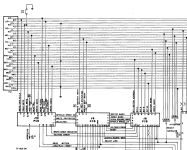
with the interface hardware, see picture attached. I'm missing some information
and I currently do not have access to a working RK05 disk drive.
-I can't find any information about the pinout assignment of the RK05 backplane.
A description of the RK05 interface cable is available in the RK8-L manual,
but only of the P1 and P2 connectors and not of the RK05 backplane.
-In the PDP-11 area there is no documentation about the sector/header format,
at least I can't find any.
General notes:
Of course it is also an open source project and I can also publish the existing
beta version on GitHub and on my homepage if required.
I am planning(!) a new PCB concept with a friend. It should consist of 2 parts.
Part 1: A general level converter from/to the FPGA world. In the beta version,
I used the https://www.sparkfun.com/products/12009 , see picture attached.
Part 2: Individual design for the RL02/MFM/RX and RK05 emulator interface which is
plugged on the level converter interface.
Another problem is the availability of the edge connectors.
Maybe it's too wasteful (for me) to develop a new PCB board. Anyway, I will try
to finish the prototype like in the picture and I will try to finish the
prototype like in the picture. Another idea: We could then send this prototype
around and everyone can save their RK05 cartridges.
My view: it should also be our joint design
In the TTL world I use the chip 74LS07, open collector and a resistor network
for the input signals. This is correct for emulator mode, but if the interface
board should also to be used as a reader only, things are different, like in my
MFM or RL02 emulator.
Help from you is necessary and every hint is also very welcome.
Reinhard
existing projects, the RL01/RL02 and MFM disk emulator, and will be also based
on the DE10-Nano FPGA board. The firmware and the associated C program is almost
ready. Everything is based on Quartus version 22.1. However, I have problems
with the interface hardware, see picture attached. I'm missing some information
and I currently do not have access to a working RK05 disk drive.
-I can't find any information about the pinout assignment of the RK05 backplane.
A description of the RK05 interface cable is available in the RK8-L manual,
but only of the P1 and P2 connectors and not of the RK05 backplane.
-In the PDP-11 area there is no documentation about the sector/header format,
at least I can't find any.
General notes:
Of course it is also an open source project and I can also publish the existing
beta version on GitHub and on my homepage if required.
I am planning(!) a new PCB concept with a friend. It should consist of 2 parts.
Part 1: A general level converter from/to the FPGA world. In the beta version,
I used the https://www.sparkfun.com/products/12009 , see picture attached.
Part 2: Individual design for the RL02/MFM/RX and RK05 emulator interface which is
plugged on the level converter interface.
Another problem is the availability of the edge connectors.
Maybe it's too wasteful (for me) to develop a new PCB board. Anyway, I will try
to finish the prototype like in the picture and I will try to finish the
prototype like in the picture. Another idea: We could then send this prototype
around and everyone can save their RK05 cartridges.
My view: it should also be our joint design
In the TTL world I use the chip 74LS07, open collector and a resistor network
for the input signals. This is correct for emulator mode, but if the interface
board should also to be used as a reader only, things are different, like in my
MFM or RL02 emulator.
Help from you is necessary and every hint is also very welcome.
Reinhard


 It has some schematics at the end of the manual, but I couldn't find the drive select circuit.