• Please review our updated Terms and Rules here

RK05 disk emulator

Did a short study of Unibus cables used to connect RK05 drives. Clever plan by DEC for reuse of cables. As suspected, not all of the signals in a BC11A are needed to connect RK05 drives.

Compared the RK05 pin assignments with Unibus, and then added the M993 adapter and M930 terminator to see how this all fits together.

Found some interesting details that are described in notes below the table in the attached summary.
1. Some pins are grounded on the M993 adapter that are not connected in the RK05, which seem to only short termination resistors to ground. No harm to doing so but seems to serve no purpose.
2. The M993 adapter connects some pins of the RK05 to RK8E (M7106) that appear to be unused at both ends.

I re-discovered (found it once and forgot :) ) Roland's clone of the M993: https://github.com/Roland-Huisman/Digital-M993-RK05-connector-board/tree/master
I was planning to design one but now there's no need... can just build some of these.
This adapter is useful in two ways:
1. for the original purpose to connect an RK05 drive to the RK8E controller.
2. as a BC11A replacement to connect two RK05 drives in a daisy-chain. Doesn't work for Unibus but should work fine to connect RK05 drives.
Simply connect two M993 boards together using a pair of 40-pin flat cables.
M993 used as BC11A.jpg
 

Attachments

  • RK05-and-Unibus-signals_v00.pdf
    1.8 MB · Views: 11
Just getting started with debugging. FPGA and SPI flash memory are soldered. The unit is strapped (via a temporary Verilog modification) to be always selected to simplify debugging to enable the outputs, because the drive isn’t actually “ready” yet. (RK05 outputs are enabled only when the unit is selected and the drive is ready.)

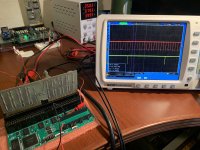
Photo showing the emulator and M930 bus terminator, lower left, with the Bus sector and index pulses on the scope screen. 40ms between index pulses which is 25 Hz or 1500 rpm.
IMG_9892.jpg

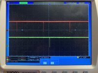
A closer look at sector and index, 2500μs between sector pulses, the index pulse is delayed by 600μs from the sector pulse.
IMG_9893.jpg

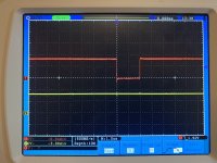
Sector pulse, 2μs width. A close-up of the index pulse looks the same.
IMG_9895.jpg

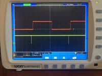
Bus sector counter bit 3 on Ch1 with index pulse on Ch2. These are active low signals so when the sector counter bit 3 is high it’s a zero and low is a one. The index pulse occurs in sector 15 so that’s why we see a delay from the index pulse to the sector counter bit 3 transition to zero (high).
IMG_9896.jpg

Looking at the DRAM pins I can also see the DRAM controller inside the FPGA is running continuous refresh cycles, which is supposed to happen when there are no read or write requests.

The RPi Pico module isn’t plugged into this board but it’s been running on another board before the FPGA was soldered. Simple test programs were run to test the microSD file system, I2C display module, serial i/o to USB and async serial pins, PWM code to drive the servo motor, and simple GPIO stuff.
 
Last edited:
Received more parts of the emulator and am now able to put much of it together. Also have been working on a tester, which is more important than I originally realized. It's the same concept that @PDP11GY described, use the emulator platform as a tester. The RK05 bus has 20 inputs and 18 outputs so most of the hardware is already there. I wish I'd put another SN75452 package on the emulator to have 20 in and 20 out. Decided to use a dipswitch on an external board to implement part of the drive select signaling while I'm short 2 driver outputs on this board. On rev 2 the extra SN75452 can be added. I'm thinking that maybe a configurable drive tester/disk reader-copier might also be a useful device. That isn't where I started though.

So, some photos... views of the front. With about 1/3 the width and height, there's not much room for anything but switches and lights.
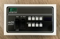
IMG_9946.jpg IMG_9943.jpg
It's intended to behave as much like a real RK05 as possible, just smaller. Run/Load switch does the same, it loads and unloads the microSD. WT PROT is momentary and works like the original, too. A small servo motor moves the microSD away from view so it can't be removed while running. There's an empty hole there right now. The microSD carrier is almost complete and prototyped but I don't yet have a nice one to install. All 8 lights indicate the same as an RK05. The Fault light is white on this one. I'm considering the purchase of a reel of translucent red filament for the Fault light diffuser but it might take forever to use all of that filament. Maybe white is okay. The diffuser block is printed as all 8 together in a frame and it's easy to cut one out and install a red color diffuser in the upper right corner. The small display to the right of the lights indicates the drive number as 0 through 7 or 0/1 through 6/7 for the "RK05f" version. Also short-duration messages will appear in the display while loading and unloading, and errors if the microSD has bad files, can't be read or isn't inserted, etc.

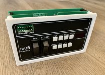
There's a 4-position piano-style dipswitch on the board just behind the front panel. You can see the "Device Select". Dipswitches just arrived this evening, haven't installed them yet.

IMG_9944.jpg IMG_9945.jpg
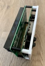
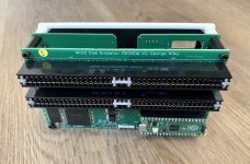
Side view on the left, the front panel electronics board can be seen. Rocker switches are quite deep and there are cutouts on this board for the switches to poke through. The main emulator board is on the back of the stack. The white bezel is 3D printed and holds everything together. M3 threaded inserts are heat staked into the four posts on the corners of the bezel.

IMG_9941.jpg IMG_9942.jpg
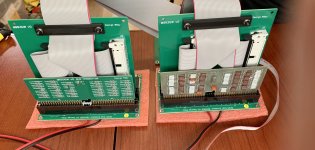
Each photo shows a tester cabled to an emulator. Almost the same hardware for each, I'll explain. Photo on the left shows the two standard RK05 slots, one with a terminator and behind that is an adapter board with cables. This is almost like the M993 but with 40-pin header connectors and with an adapter board at each end can be used to extend the RK05 bus to additional drives. There's a little non-standard thing with the BUS_RK11D_L signal so it can also extend to more drives in a PDP-11 system that use the binary encoded drive selection method. The black flat-cable clamp is a 3D printed piece... quite simple. This doesn't have all of the Unibus signals but does have all RK05 signals. The pinout of the two 40-pin cables is also set up to plug into an RK8-E controller. I see that the RPI-Pico is currently missing from the tester board... not intended.

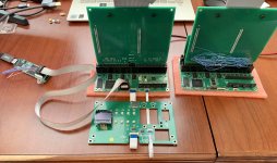
The photo on the right is the other side of the configuration seen on the left. The board on the left of the right-hand photo is the emulator and the board on the right with the blue-wire rat's-nest is the tester. The blue wires route the drivers on the tester to signals that are receivers on the emulator, and vice versa. This is the only blue-wire version that I'll ever make. If there's interest in a drive tester then a PCB will be designed. The board in front with 3 holes in it is the front-panel electronics which connects to the main emulator board via a 20-pin flex. There's also a tiny 8-pin flex that connects from the emulator to a microSD socket that's on the front panel. This microSD on the front panel is just something for the prototype so I'd have a way to connect a micoSD for debugging. The next version of the front-panel electronics will have this socket and flex connector removed and they'll be on a separate tiny board that mounts to the microSD carriage that tilts out of the way when the "disk" is loaded.

Just recently completed design and unit testing of the Verilog for the tester FPGA. It'll be fun to pair this with the emulator. In a prior post there were scope traces of the emulator generating sector and index pulses, but now we get to more fun stuff with reading and writing data, confirming the disk read/write timing and CPU interface.
 
Wow - I am very impressed by your work!!!
Once finished are you planing to release this as a kit or a fully assembled unit?
I would love to buy at least 4 if you do.
Thanks, Tom. Definitely plan to make all of the documentation available on github. Haven't yet decided whether to make kits or assembled units available. While building it I realized that some assembly steps are rather difficult for anyone to do in their garage. The emulator main board, front panel electronics and front panel were all made by JLCPCB to avoid having to do SMT assembly. That is, except for the 144 TQFP FPGA. They had none in stock and I didn't want to wait for parts consignment so I soldered them myself. Maybe kits made up of assembled boards would be do-able. I'll need to think about that.
 
I think the tester and disk readers are both worthwhile projects, especially if the reader could be extended to
handle flux dumps of different kinds of packs.

I'd finally be able to retire my old Wilson Diablo drive tester.
 
I think the tester and disk readers are both worthwhile projects, especially if the reader could be extended to
handle flux dumps of different kinds of packs.

I'd finally be able to retire my old Wilson Diablo drive tester.
Thanks. Tester and reader are the same device. I need a tester to be able to thoroughly verify the RK05 emulator. While designing the FPGA for the tester it was easy to make the various field lengths configurable which could be useful for emulator verification. This would also allow the tester/reader/copier to be configurable for many different sector sizes.
 
Received more parts of the emulator and am now able to put much of it together. Also have been working on a tester, which is more important than I originally realized. It's the same concept that @PDP11GY described, use the emulator platform as a tester. The RK05 bus has 20 inputs and 18 outputs so most of the hardware is already there. I wish I'd put another SN75452 package on the emulator to have 20 in and 20 out. Decided to use a dipswitch on an external board to implement part of the drive select signaling while I'm short 2 driver outputs on this board. On rev 2 the extra SN75452 can be added. I'm thinking that maybe a configurable drive tester/disk reader-copier might also be a useful device. That isn't where I started though.

So, some photos... views of the front. With about 1/3 the width and height, there's not much room for anything but switches and lights.
View attachment 1259049 View attachment 1259050
It's intended to behave as much like a real RK05 as possible, just smaller. Run/Load switch does the same, it loads and unloads the microSD. WT PROT is momentary and works like the original, too. A small servo motor moves the microSD away from view so it can't be removed while running. There's an empty hole there right now. The microSD carrier is almost complete and prototyped but I don't yet have a nice one to install. All 8 lights indicate the same as an RK05. The Fault light is white on this one. I'm considering the purchase of a reel of translucent red filament for the Fault light diffuser but it might take forever to use all of that filament. Maybe white is okay. The diffuser block is printed as all 8 together in a frame and it's easy to cut one out and install a red color diffuser in the upper right corner. The small display to the right of the lights indicates the drive number as 0 through 7 or 0/1 through 6/7 for the "RK05f" version. Also short-duration messages will appear in the display while loading and unloading, and errors if the microSD has bad files, can't be read or isn't inserted, etc.

...
Any news on this project George?
 
Any news on this project George?
Thanks for asking, Tom. I've been away at a conference for a week+ so progress has been slow since the last update. Mostly have been testing and debugging the FPGA code in the emulator tester. Wrote a simple debug monitor that runs on the RPi Pico to be able to read and write any register in the SPI space. There are lots of registers defined in the FPGA code for configuration and catching errors, so the monitor program is quite useful for debug and test. Working on an SPI read problem now... I think its' just a matter of clocking the serial read data on the proper edge.

The FPGA process has been to use Xilinx Vivado for the development environment and behavioral simulation, then switch over to Lattice iCEcube2 for synthesis, placement & routing and generating the config memory bitmap. This is fairly seamless, actually. Just have both tools running, save the Verilog files while in Vivado and start the P&R process in iCEcube2. (I hope Xilinx and Lattice tools aren't aware of each other running concurrently :ROFLMAO: ) Talked to a guy from Lattice while at the conference last week and as a result looked a bit into using the Lattice Edition of Mentor Modelsim for the front end so I'd be completely within the Lattice toolset. Decided to stick with the present setup, I really like Vivado.

I'm learning that being able to pack so much logic into an FPGA of this size brings the challenge of having to verify a lot of functionality. Even though all of the Verilog modules have been unit-tested in behavioral simulation it still takes more time than I imagined to confirm the functionality at the system level, when it's all put together running on the real hardware.

So far, many of the SPI write bits have been verified, reading has an issue - read data is shifted right one bit probably due to the clock edge. Sector and Index pulses in the actual RK05 emulator are working (tested only 16 sector mode). None of the DRAM read/write logic has been verified yet, although the refresh timing appears to be correct. Haven't yet done any debugging/testing with the emulator and tester connected together. The tester-to-emulator cable is built and ready to use when both sides have been verified independently. The modern M930 SMT terminators seem to be working well and have also been verified using a resistance check.
 
Last edited:
here are the timing specs for the diablo sync fields in a sector
header and data and bit order in the sector data are dependent on the format implemented by the controller
the information manual on the model 30 mentions 8-24 sectors are supported
quickly looking, i've seen 8,12,16 and 24 sectors used by various systems. 12 is used on pdp-11s, 16 on pdp-8s
Have been able to document in much detail the 16-sector format used by the DEC RK8-E and 12-sector formats used by the RK11-D and RK11-E.

I'm eager to learn the details of other sector formats used by controllers that would attach to a Diablo model 30 series drive, particularly the 8-sector and 24 sector formats mentioned.
By knowing this, the tester could be configured to read and write these other formats.

The tester and emulator have been designed to have configurable lengths of fields such as Preamble, Data, CRC and Postamble. The Header length could also be configurable with little effort.
Maybe these other disk controller formats have additional fields? And is there always a single Sync bit that follows the Preamble?

Pointers to any documentation would be helpful. I tried to browse Bitsavers but there's just so much information it's difficult to search for which controllers use these particular drive types.

I was at CHM last month and saw what looked like a Diablo model 31 connected to a Xerox Alto: https://www.computerhistory.org/revolution/input-output/14/347
Would it be useful to read or write Alto disks?

In the CT Scanner photo on this Nova page in Wikipedia it looks like a Diablo model 31 connected to a DG Nova 1200.
 
Last edited:
It would be useful!
The Alto disk format is documented in the hardware manual.
It is a 12 sector pack with a slightly faster clock and a longer data block to include a tag field
Hey, thanks! Section 6.0. And there appears to be an additional field called the Label Block. So, the Emulator and Tester need to have no awareness of any fields past the Sync bit. That’ll be an easy update and reduces complexity of two state machines.

If the faster clock is 1.6 Mbps that’s a lucky number given the present 40 MHz system clock, just a perfect divide-by 25.

The RK05 bit clock is 40 MHz divided by 28, which is 0.8% slow (1.4286 actual compared to 1.44 ideal) but well within the RK05 rotation speed accuracy.
 
In the CT Scanner photo on this Nova page in Wikipedia it looks like a Diablo model 31 connected to a DG Nova 1200.
Yes, DG supported the Series 30 drives. That photo looks like a 6045 Cartridge Disc Subsystem. Attached are what I believe are the only two documents available describing that subsystem. See page 10-of-91 in the first document for the basic specs: 408 cylinders, 4 surfaces, 12 sectors (512 byte).
 

Attachments

  • 015-000057-02 6045 Series Cartridge Disc Subsystem.pdf
    3.8 MB · Views: 4
  • 015-000058-05 6045_6050_6051 Cartridge Disc Subsystem.pdf
    4.3 MB · Views: 7
Yes, DG supported the Series 30 drives. That photo looks like a 6045 Cartridge Disc Subsystem. Attached are what I believe are the only two documents available describing that subsystem. See page 10-of-91 in the first document for the basic specs: 408 cylinders, 4 surfaces, 12 sectors (512 byte).
Note that the drive consists of a fixed disk (5MB, below) and a removable IBM 5440-type cartridge (5MB, above).
 
Yes, DG supported the Series 30 drives. That photo looks like a 6045 Cartridge Disc Subsystem. Attached are what I believe are the only two documents available describing that subsystem. See page 10-of-91 in the first document for the basic specs: 408 cylinders, 4 surfaces, 12 sectors (512 byte).
Thanks Paul, that's an interesting disk format. It appears to have a detailed address field that contains both cylinder and sector addresses slightly separated from the data field by a splice. Kind of implies the data can be written separately and the addressing information can remain.

The photo I was referring to is two photos below that one in the Wikipedia page, "A Nova 1200, mid-right, processed the images generated by the EMI-Scanner, the world's first commercially available CT scanner.":

I'd be interested in the Data General disk controller for that configuration.
 
Thanks Paul, that's an interesting disk format. It appears to have a detailed address field that contains both cylinder and sector addresses slightly separated from the data field by a splice.

the same controller is used for hard and floppy disks.
 
Back
Top