• Please review our updated Terms and Rules here

SBC interest?

If this is an educational project, what level of functionality should it have? It's pretty easy to design a simple machine that has only 256 bytes of memory, for example. As the data and address paths get wider, the design gets more complex.
 
If this is an educational project, what level of functionality should it have?
I was mulling that question over today. It'd be great if you could actually do something useful with the end result; I think a purely educational CPU would quickly end up gathering dust otherwise. Is a 4-bit architecture going to end up being just too limited? Moving up to (say) 8 bits would indeed make things a lot more complicated, but you'd also be able to do a hell of a lot more with the thing. A few K of address space would also make the difference between a fun educational tool and something resembling a "proper" computer.

One concept that popped into my head (and I'm really not sure if this falls within the realms of people's expectations regarding how far this thing should go) is that of some kind of cut down PDP-11-alike. The real thing is just about understandable for one person and although a TTL implementation is a good few board's worth of parts, maybe an 8-bit adaptation with less registers and features would be manageable enough.
 
A lot of legacy microcontrollers have very limited functionality and still manage to do something worthwhile. There were arcade games that ran from a Rockwell PPS-4, for example.
 
A lot of legacy microcontrollers have very limited functionality and still manage to do something worthwhile.
Good point indeed. I guess you could do 4-to-8 bit instructions, multiplex out a 12-bit address bus - something like that? Then again, if you're going to end up multiplexing everything, maybe it's simpler (and clearer design wise) just to use wider data paths. At least with 8 bits you can push ASCII around easily. Double it up and you've got a very generous address space for a small processor, some of which you could use for I/O.
 
I was wondering if there might be any interest in creating a single board computer (SBC) that is basically VC forum designed and supported?

[snip]

Hi All! It appears this project has either fizzled or radically departed from the original posters comments. If you are interested in building your own home brew computer, you are always welcome at the N8VEM home brew computing project. I much appreciate the support the Vintage-Computer.com community has shown to the N8VEM home brew computing project several months ago. It has been very good and helped bring easy access to home brew computing to many hobbyists.

The N8VEM project certainly has a lot of room for improvement but it does offer a lot to home brew computing enthusiasts. Primarily, it is a solid foundation of tools and infrastructure for building new systems and peripherals. The current SBC is a Z80 CP/M system which is a great place to start but you are not restricted to it. Those areas for improvement are great opportunities for new builders to contribute. All sorts of things from new hardware, software, writing documentation, web design and maintenance are all needed and much appreciated by friendly and robust community.

The N8VEM dual approach allows either standalone SBC or a bus based system that gives a lot of flexibility. For example, the ECB backplane and other peripherals could easily be incorporated into another SBC using a different CPU such as an 8088 or 68K. I am currently developing a 6809 host processor that is nearing its PCB manufacturing order so it is certainly possible. Alternatively, you can build peripherals directly on the SBC as several builders have done or boards for the ECB backplane.

All the PCBs are available so if you would like to participate please contact me and let's get started! I've tried to keep the costs low as possible and still able to sustain itself. All the information for hardware, software, and documentation is publicly and freely available.

http://groups.google.com/group/n8vem

http://n8vem-sbc.pbworks.com/

Thanks and have a nice day!

Andrew Lynch
 
help...cpr...cpr...

help...cpr...cpr...

I hope this thread hasn't eneded up where I had previously
mentioned it might end up!!!

1- Forget about functionality!!!
2- Let's stick to educationality...
3- How about a tutorial on CPLD, JTAG, and a few simple examples?

What is important is Live Tech-Support and question/answer.
Let's start doing something fun...

And Thank you for your support

ziloo :biggrin:
 
Last edited:
As far as CPLD (and other programmable logic) goes, there are tons of Verilog tutorials on the web. Just Google "Verilog tutorial" or "learning Verilog". (There are other languages (e.g. VHDL) used to write functional descriptions for programmable devices, but Verilog is perhaps the easiest).

CPLD is the little brother to FPGA--you can do whole systems in FPGA; CPLD limits itself to a much lower number of cells. On the other hand, CPLD is ready to go as soon as power is applied; FPGA requires that the programming be loaded (either from on-chip flash or an off-chip source) before the device is ready to use. The design software is usually available free of charge.

I think CPLD represents a happy medium between discrete TTL logic and FPGA. Complex enough to simplify the implementation of a design, but not so complex that the implementation seems like a "black box".

There isn't too much to say about JTAG, other than it's a serial protocol used to program and debug devices. It's not unusual to see a JTAG programming setup used as both a programming interface and as a debugging interface. The big advantage of JTAG is that a device can be programmed while soldered into the circuit in which it's being used. Need to fix a bug? Just modify your program and blast it in. No hot soldering iron needed. JTAG programmers, if you have a parallel port on your PC, are very easy to make.

JTAG's all over the place nowadays. It's in modems, routers, mobile phones, MP3 players, DTV set top boxes....you name it.
 
What is the smallest logic element of a CPLD? I know about
PALs and GALs and their smallest element which we actually
burn to program them; But in programming a CPLD, what is it
that we are doing to create the logic we desire?

ziloo
 
Exact CPLD implementation varies between vendors, but a fairly typical device and the way it works is the Xilinx XC9500 series. This a 5V series of CPLDs that can be had in 44 and 84 pin PLCC packages (they'll go into a socket with 0.100 lead spacing). Altera offers a similar 5V family the MAX 7000 series.

Newer devices are 3.3V, rather than 5V and tend to be offered in surface-mount packaging only.
 
Our orginal poster seems to have gone quiet for a bit. Scorch, are you there??

Anyway, sbc stuff is evolving rapidly. I posted a reply a few weeks ago with this:

"Hardware:
...
Almost: SD or CF card interface"

Well, we now have mass SD storeage on the N8VEM. (Thanks++ to all those who answered my esoteric questions on CP/M fdos handles etc. There was a real and practical outcome). 2Gig of file storage designated as "Drive U" on the N8VEM. So it now has drive A as a battery backed ram disk with 448k, Drive B with 16k of ROM drive for essential bootup files (Xmodem etc), and Drive U with 2,000,000,000 bytes (2 million k!!) of storage. That is more than enough to contain every CP/M file ever written!

Incidentally, if any vintage computer owner on this forum wants mass storage, all you need is a spare serial port, and the OUT and IN port locations for that serial port. The uDrive assembly and .COM programs are all open source over at the N8VEM group and I'd be happy to assist anyone get it working on another type of machine.

I can solder one of these boards in 40 minutes so it ought to be well within the capabilities of high school students. And not many SBC projects can go from a pile of chips to a self contained computer playing chess in 40 minutes. (And the program continues to beat me on the easiest level. Darn this new-fangled artificial intelligence...)

Further, the guys over at the Propeller forum are working on shrinking the N8VEM and getting it down to only 3-4 chips. That ought to make it quicker to build, and cheaper and smaller and able to use less power.

Thanks to the invaluable help here, there now exists a SBC with ample storage and all running pukka, vintage, CP/M. So, in a round about way, the Vintage Computer Forum *is* working collaboratively on building a SBC...
 

Attachments

  • uDrive_N8VEM.jpg
    uDrive_N8VEM.jpg
    96.7 KB · Views: 1
Exact CPLD implementation varies between vendors, but a fairly typical device and the way it works is the Xilinx XC9500 series. This a 5V series of CPLDs that can be had in 44 and 84 pin PLCC packages (they'll go into a socket with 0.100 lead spacing). Altera offers a similar 5V family the MAX 7000 series.

Newer devices are 3.3V, rather than 5V and tend to be offered in surface-mount packaging only.

Hi Chuck! Thanks!

A hobbyist could easily use the N8VEM system to create a CPLD peripheral in 0.100" lead spaced packages (DIP, PLCC, PGA). Just use the existing and available ECB prototyping board to mount the device. There are a bunch of compatible devices at Digikey using 5V which would require minimal interfacing and even 3.3V devices if one used a local regulator onboard. I think it would be ideal for educational purposes and I have been advocating the N8VEM project for education since the beginning.

At least at first, you could just use power and ground and physically mount the device on the ECB prototyping board and use JTAG or whatever interface it has. Directly interface a CPLD to the ECB it would require about 11 IO pins I think assuming; a chip select, a /WR signal, a register select (A0), and 8 data lines. It could probably be done in fewer if needed. Especially using the 68 pin PLCC or larger packages they certainly have enough pins left to be useful. Alternatively, one could use a 8255 as an interface between the CPLD and the ECB. There are many options!

I like the 28, 40, 44, and 68 pin devices since those are really easy to work with as wire wrap sockets are available. Depending on how its interfaced, using a since CPLD would leave most of the 4"x4" prototyping area left for whatever else the builder wants to include. One N8VEM builder is doing exactly this right now to interface a Propeller chip. The Propeller is more of a microcontroller than programmable logic device but a similar approach could be used to easily interface a CPLD to the ECB.

The same probably applies to FPGA devices in the 44, 68, and 84 PLCC packages especially the 5V compatible versions. Digikey has several in stock from FPGA manufacturers. I supposed the PGA packages as well although the problem with larger sizes is there aren't wire wrap sockets available (although you could make your own using machine pin SIP sockets) and current draw gets to be problematic at larger sizes. I'd bet that all the PLCC packages are practical though.

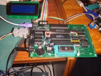
The N8VEM system is intended to be a platform for expansion with home brew peripherals. It is easily done. I have built several peripherals and builders are making more all the time. Just recently some builders are making a keyboard display front panel like device and more are on the way.

All through the N8VEM home brew project development I've kept the hobbyist in mind using low cost, reliable, and easily assembled components. I'll agree its not the most advanced or powerful system available but every builder I know of who has started their system has finished with a working system -- usually on the first try. Having the CP/M environment is free, simple, and familiar enough to use right away.

Yes, you could use a PC or another prototype board but where is the fun in that? :) There are some people I'll never convince and that's OK. For those who'll listen I'd like to encourage hobbyists to build on what's already available N8VEM home brew system there rather than start from scratch. It is a *lot* easier to leverage an existing system and may have long term benefits that'll continue to help the community when it's done.

Thanks and have a nice day!

Andrew Lynch, 73 de N8VEM

PS, I just ordered PCBs for the N8VEM 6809 host processor board and they should be available soon. The only software that runs on it at the moment is hacked version of the Motorola MiniBug. Further development of the 6809 side of N8VEM would make a great hobbyist project. There are some 6809 operating systems and applications freely available like FLEX and CUBIX just waiting to be ported.
 
Last edited:
Hi Andrew,

Yesterday, I started thinking about an interesting idea. Bear with me--this is still nascent.

What about a "universal microprocessor"? Most people on this list have not had an opportunity to explore some of the more obscure vintage microprocessors, such as GI CP1600, National SC/MP or PACE, Fairchild F8 or 9440, etc. Given the scarcity of vintage parts and the problems involved with interfacing them (e.g. MOS-to-TTL translation, multiple power supplies, etc.), it's not worth doing more than a one-off on perfboard, if that.

However, if one were to take a respectably speedy microcontroller (maybe an ATMega16 or 128 or whatever the PIC version of that is), some SRAM and a CPLD for interfacing, one could emulate just about any microprocessor one wanted. Put a JTAG header on for both the uC and CPLD and make whatever you want. Except for some CPLD tinkering, no need to learn VHDL or Verilog. Most larger uCs have built-in UARTs for debugging. Make up your own instruction set if you'd like.

Pick your architecture, flash the code and you're off and running.

What do you think?
 
Hi! I think people are doing exactly that with FPGA designs and protoboards like the Xilinx Spartan III etc. Sure it can be done but the hard part is not the hardware since that is basically fixed COTS. Its the logic in the Verilog/VHDL that captures precisely the characteristics of the legacy CPU and blows it into FPGA flash. I believe the Z80 has already been done with the T80 project and probably 6502 etc. Certainly "doable"

I guess I just find using an off the shelf circuit board loaded with fine pitch SMT parts rather unappealing from a home brew perspective. To me that's not much different that just buying an off the shelf PC from WalMart. My interests are more building something from scratch and using it. There is something just very satisfying about creating something from a pile of components that off the shelf units can never match.

Probably your idea could be implemented using a high end CPLD or low end FPGA mounted on an N8VEM ECB prototyping board assuming the chip has enough capacity for CPU emulation. If it were sophisticated enough it could be ECB bus master and then you wouldn't need the N8VEM SBC at all but at the cost of using about 36 IO pins. The approach I am advocating relies on the CPLD/FPGA appearing as a peripheral (IO ports) on the ECB in the Z80 IO address map which would be more simple, I think, and require only about 11 pins.

What you suggest is very likely possible, I just don't know. The things I've found with the various ECB peripherals I've built so far indicates it probably is possible. Certainly I think interfacing a CPLD/FPGA as a peripheral is possible as that's how I am doing the 6809 host processor and Dave is building the direct ECB to Propeller IO board. I built an ECB UART to Propeller peripheral myself a few months ago and it was super easy. It is a small leap from there to the CPLD/FPGA board, IMO.

I think the main advantage of making the device part of the N8VEM home brew project though is its able to leverage whats already available and it is placed into a context of other similar projects. There are *lots* of home brew projects around but almost all of them are one-offs stand alone units. Basically you can observe them but in order to make your own you are essentially recreating the entire project. With N8VEM, you can build what you need from PCBs (SBC, ECB backplane, and ECB prototyping board) and then focus on the essential part you are most interested in, such as a CPLD/FPGA peripheral, without "reinventing the wheel" everytime or creating yet another isolated home brew project.

You are probably the special case though since you have such a vast amount of real world experience, are extremely knowledgeable on these matters, and have the resources to back it up. However, for (casual, average, regular) hobbyists I think the appeal of leveraging an existing home brew system would be significant.

There is one way to find out for sure though... build a system and find out. Few things are more convincing than a working prototype! Real hardware beats great sounding theory any day!

Thanks and have a nice day!

Andrew Lynch

PS, my current project is building a Video Display Unit for the N8VEM. I am interfacing a SY6545 on an ECB prototyping board. The plan is to make a simple character mode composite video board like the KayPro 10 and probably a simple PS/2 keyboard interface. I've got the prototype about 50% done with wire wrapping. There are pictures in the N8VEM wiki page under the "VDU" folder. I am not sure what I am going to do next after this board. It depends on how Dave's ECB Propeller board turns out -- we really need that Propeller IO board IMO; VGA video, PS/2 keyboard, mouse, audio, SD... what's not to like!
 
Last edited:
Hi Andrew,

I think my outline was perhaps a little misleading. The CPLD's only purpose is to minimize the ancillarly logic between the memory and the bus--it could just as well be implemented as random TTL.

My object here is to make emulation easy. Writing miles of VHDL to implement something on the scale a Z80 or 6502 in FPGA is a tough time-consuming job with all sorts of issues relating to timing and getting things "just right".

On the other hand, a lot of people can write C or assembly, so coding an emulator for, say, a Z80 is no great feat (I feel qualified to say that. ;) ) So, instead of an FPGA, one uses a microcontroller interfaced to external memory and writes an emulator for whatever processor in whatever language.

Want to move from a Z80 to 6502? Write a new emulator for a 6502 and download it into the uC, without removing anything from the system.

You could certainly interface it to your bus, particularly if your bus supports a 16 bit data path.

While there may be a certain romance to scrounging old parts, I think a more up-to-date and easier to work with implementation might be more attractive.

PLCC CPLDs are still available and DIP versions of microcontrollers remain popular. Even if one had to use a QFP version, inexpensive adapter boards to 0.100" spacing are easy to find.
 
Hi Chuck! Thanks, oh, I see. Yes, that is a bit different than what I was talking about. The beauty of the uC/SRAM combination is it can be a form of "generic" or programmable IO. The SBC CPU can communicate with it easily through the ECB and interface logic whether that's a CPLD or simple buffer/decoder logic is just implementation.

What you are describing is similar, IMO, to the N8VEM Propeller board Dave is working on. The N8VEM SBC communicates with the Propeller directly as a peripheral by accessing it as a port through buffer/decode logic. The remaining pins of the Propeller are used for a variety of IO tasks like VGA, PS/2 keyboard, etc. However, with Dave's board the IO pins are dedicated to specific tasks and are no longer available for use.

As an extension of the principle and probably more along the lines you are describing is to just keep the Propeller's IO lines available by exporting them to a connector of some sort like a 40 pin DIP socket. Then the builder adds the devices they want to include CPU or other device emulation. The concept is readily extended to FPGA like devices as they are fully programmable and have lots of available pins.

The major shortfall of using a Propeller or any 40 pin uC in this application is the number of available IO pins. Say it starts with 32 IO pins but by the time you subtract the serial IO (2), EEPROM (2), and ECB interface (11 or more) your are down to 17 unallocated pins which is not enough to directly emulate any CPU larger than a 4004. That's where larger uC or FPGA's additional pins would really shine.

Hopefully Dave's board comes to pass as that will be an interesting and useful device. Since it is directly accessed as an IO port, I believe it will be quite fast as well. It should be much faster than going through a UART or PPI as an intermediary. My prototype used a UART for interfacing and was 9600 bps since the CPU polled its IO which limited performance.

Certainly there are many opportunities for the interested and motivated hobbyist. I guess we'll see if anyone picks up the "bug" and goes forward with implementation.

Thanks and have a nice day!

Andrew Lynch
 
Back
Top