• Please review our updated Terms and Rules here

SuperPET 64k RAM Expansion DIMM Troubleshooting

miraco

Experienced Member
Joined
Mar 13, 2015
Messages
81
Location
US - Louisville
Hello everyone, I am attempting to resolve an issue with the upper 64k ram in my SuperPET. I have a Basic program that cycles (slowly) through the banks to identify the bit(s) and bank(s) at fault. I am currently unable to determine how the banks map to the physical array of 32 2k memory dimms. This is a 3 board SuperPet. I am running the Basic diagnostic program from the 8032 side, which doesn’t exhibit any issues. Also is it possible to piggyback 4116 dimms for troubleshooting?

Thanks for any help and/or suggestions!
 
If you PM me your email address I have what I think is the official the superpet burnin programme (machine code) that identifies the ram which may help
 
The first thing to say is that a 4116 is a 16Kbit * 1 bit device - not a 2K[byte] device. This means that eight ( 8 ) 4116 devices are required to form a byte.

I have worked on the single-board SP9000 - so I am somewhat rusty on the 3-board setup. But, if memory serves me correctly, the following is likely to apply:

Banks 0 and 1 = U29-U36.
Banks 2 and 3 = U37-U44.
Banks 4 and 5 = U45-U52.
Banks 6 and 7 = U53-U60.

The lower-numbered device of each block of 8 chips (i.e. U29, U37, U45 and U53) being the most significant data bit (DB7) with the higher-numbered device being the least significant data bit (DB0) (i.e. U36, U44, U52 and U60).

One of the 8 banks is mapped into the address space $9xxx depending upon the setting of the bank switch register (the least significant 3 bits).

You also have to remember that testing RAM when it is set to READ-ONLY doesn't work - and neither will it work if the switch is set to PROG and the bank switch register set to WRITE-PROTECT either.

I would first check all of the power supply rails to make sure they are within specification (+/- 5% of rated voltage at most). So (for the +5V rail) that should be 4.75V to 5.25V. If you have an oscilloscope - check for ripple and high frequency noise.

Are your 4116 DRAMs in sockets? If so, I wouldn't bother about piggy-backing. Just buy eight spare devices from a reputable supplier and swap an entire block of 8 devices over. If those two banks now work - you can selectively replace (say) DB0 from that block with an unknown device and see if that returns as FAULTY or not. Divide an conquer.

Can you point me to a copy of the test program you are using?

The other thing of note is the horrible 'analogue' logic around U26 - and C76. Timing circuits are notorious for drifting with age and (because this is the refresh and /RAS signal generation) could cause memory access problems.

You might also want to consider a little 4116 DRAM tester that you can buy? 4116 DRAM is notoriously unreliable. Piggy-backing (in my opinion) is generally inconclusive - but I have known it to work once or twice and is a preferential test before desoldering and replacing a device... If it is in a socket though, I wouldn't bother. However, whatever you do, make sure it is methodical and you keep notes. There is nothing worse than trying to find a pattern and then forgetting where the devices are that you first started with! If you start swapping devices around, at least put a sticker on each device to start with stating which 'U' device it is!

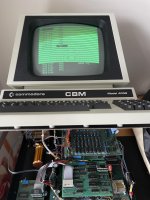
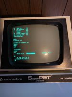
You also haven't stated what problems you are actually observing...

Dave
 
Last edited:
Andy, I have PM'ed my email address.

Dave, thanks for the reply.

Yeah sorry, they are definitely 16k bit devices! They are not in sockets, that would be too easy ;) Do you have a suggestion concerning a DRAM tester?

The 3 board SP has a total of 16 banks. How would those map to the four 8 chip blocks?

The issue I see is that once I load a language/dev/editor from menu it will hang or return to the start menu. Just started this behavior a few weeks ago.

How would you like me to send the basic diagnostic program?

Thanks for your help!
 
I hope this comes through …. unzip the file and you get the machine code program superset burnin. Run it in standard 8032 mode and it cycles through the banked memory and identifies any bad ram. If one fails it will display the RAM locations and drop into the TIM. You can modify the code to continue the cycling rather than break to TIM with a small modification but lets see what happens first.,

Can you post pics of your board setup also and check the toggle switch is set to RAM (if one has been wired in)
 

Attachments

  • superpet burnin.zip
    1 KB · Views: 8
Last edited:
Heres an example of it running in my setup
 

Attachments

  • IMG_5056.jpg
    IMG_5056.jpg
    200.4 KB · Views: 7
Yes, I missed an address line off the bank switch register. The allocation of bank numbers to RAM blocks is not as nice and clean as it should be. It will take me a little time to work it out from the schematics. MA0 appears to have BA0 and the high bit of the bank switch register multiplexed onto it. This just complicates things for mere mortals!

Let's see what Andy's test code comes up with first.

Four things could cause your problem off the top of my head:

1. DRAM refresh not working properly.
2. /RAS and /CAS logic not working properly.
3. DRAM device faulty - or slow (leading to inconsistent results).
4. Faulty 6702 dongle device.

The latter one is interesting. Are you using the 'original' language disks or the ones that I removed the 6702 dongle protection from? If the latter - point 4 is not responsible!

Dave
 
Memory test stops quick at U53-60 (12-16k)
 

Attachments

  • photo62746.jpg
    photo62746.jpg
    117.9 KB · Views: 5
  • photo62747.jpg
    photo62747.jpg
    100.3 KB · Views: 5
Dave,

I am running with copies of my original 1.1 disks and the original 6702 dongle protection daughtercard. I will attempt to create copies of your un-protected disks if necessary.
 
Last edited:
OK lets do a little house keeping so I understand the configuration.

(1) Does the SP display the Waterloo menu when you switch from 6502 to 6809 ?
The Waterloo boot screen will also display if you disconnect the ram board.

(2) Are the toggle switches set as follows?

Toggle Switch U11 - set to off
Toggle Switch U12 - set to RAM
Toggle Switch next to the 6502/6809 - set to R/W

(3) If the RAM test still fails, when it drops into TIM, type
m 2245 2245

You will get a line of hex numbers displayed, the first will be 00 (BRK)

Move the cursor to 00 and change it to 60 (RTS) and hit return.

Type m 2245 2245 and check the number has changed to 60

Hit x to exit

Re-run the program, It will go into continuous loop of cycling through all the RAM on the board. If all the RAM fails then it is a different fault on the RAM board of 6809 board. You will have to power off to stop the test.

(4) If they do fail then check all the connection are good and you have 12v, -5V and 5V coming out of the voltage regulators on the RAM board - I am assuming you are comfortable doing this with a voltmeter, if not then leave this step out and others can talk you through it.
 
Just in case you need more information on the code change ... when it breaks into TIM

b*
pc irq sr ac xr yr sp
.; 0401 e455 32 04 5e 00 f8

Type

.m 2245 2245 <Return>

you get
.: 2245 00 4c 4c 22 20 c4 22 60
.

move cursor over the 00 and change the 00 to 60


.: 2245 60 4c 4c 22 20 c4 22 60 <return>

hit return so it is saved in memory

.m 2245 2245 <Return>

check it has changed to 60

x to exit then re-run the test
 
So I verified that the switches were in the correct position, ran the program from the 8032 side and it reported FAIL for the following:

U53-60 (0-4k)
U53-60 (4-8k)
U53-60 (8-12k)
U53-60 ((12-16k)

The other three dram blocks pass.

HOWEVER...

I now have a bigger issue. The SP had been acting flakey when first powered on and would hang until I reset with the 6502/6809 switch. This morning after I ran the diagnostic program I noticed that the screen was dark. Powering off and on gives me a dot in th middle of the screen before fading away. This happened once before but the machine recovered after several seconds!
Sounds strange I know but ...

Going in the wrong direction :(
 
Ok something is intermittently failing temporarily. The SP has decided to power up again after a couple of false starts. :confused:
 
We know that 99% of the circuitry is common between all of the RAM banks - so it is either a faulty DRAM device in U53 to U50 (perhaps AndyG can chip in (no pun intended) with the diagnostic program identification of a potentially faulty DRAM bit) or a couple of gates related to U53 to U50 alone. This is now potentially fixable. It also may be worth trying the piggy-back testing but (before you do) let's talk about how to perform this test safely.

As to the 'flakiness', does this happen mainly at power-up time? If so, it may indicate a problem with the reset circuitry. Does it only occur with the 6809 switched in or with the 6502 as well (the circuitry is common to the two CPUs).

Dave
 
I think we need to figure out the "flaky" bit first. Are all the cables plugged in OK - you can remove the ram board and it will still boot. You can also strip the SP boards out and put the 6502 back into its native socket to test the main motherboard independently of the SP boards.

With regards to the faulty DRAM, U53-U60 looks like is failing on all bits for the entire bank (I doubt all 8 are bad) so it could be, as Dave says, be related to a couple of gates - looking at pin 3 of U9 comparing it with pin 6 of U9 for example (with a scope) when running the burnin programme may show something. It could also be one dead DRAM pulling the whole bank down.

http://www.zimmers.net/anonftp/pub/c...T/324041-3.gif shows the circuit diagram where I would start to probe. As all of the IC's are soldered in it will be slow detective work.

I think having a reliable base is important therefore before we can reliably probe deeper.
 
Last edited:
FWIW this is the Basic program I was using to diagnose the dram issue:

0 p=1: print chr$(147)
1 print"{down}Bank Address 76543210"
5 print chr$(19);"Pass";p
10 for m=36864 to 40959
11 for b=0 to 15
12 poke 61436, 128 or b
15 printchr$(19);:for cr=0 to b+2: print"{down}";:nextcr
17 b$=str$(b)
18 if b<10 then b$=" "+b$
19 print b$;
30 for da=0 to 3
35 read o: poke m,o:i=peek(m)
40 data 0, 85, 170, 255
45 if o = i then goto 1000
500 rem display bad bits
505 printchr$(19);:for cr=0 to b+2: print"{down}";:nextcr
512 print b$;" ";m;" ";
515 c$="{rght}"
520 if (i and 128 ) <> (o and 128 ) then c$="X"
521 print c$; : c$="{rght}"
525 if (i and 64) <> (o and 64) then c$="X"
526 print c$; : c$="{rght}"
530 if (i and 32) <> (o and 32) then c$="X"
531 print c$; : c$="{rght}"
535 if (i and 16) <> (o and 16) then c$="X"
536 print c$; : c$="{rght}"
540 if (i and 8 ) <> (o and 8 ) then c$="X"
541 print c$; : c$="{rght}"
545 if (i and 4) <> (o and 4) then c$="X"
546 print c$; : c$="{rght}"
550 if (i and 2) <> (o and 2) then c$="X"
551 print c$; : c$="{rght}"
555 if (i and 1) <> (o and 1) then c$="X"
556 print c$;
1000 next da:restore
1005 next b:next m: p=p+1:goto 5


It shows an issue with bit 6 (of 0-7) in banks 6,7,14,15

The stability issue affects both 6502 and 6809 modes. It will usually occur soon after or during power on but also after running for a time.

I realize I will need to get back to a basic 8032 setup in order to troubleshoot the gremlin but would like to at least identify a fix for the dram if possible beforehand.

Thanks for your help.
 
Last edited:
I have to say I have not had a great experience with basic ram test programs for the superpet RAM board. When I first got mine I used one identical to yours - it isn't fast enough to stress the board and led me in the wrong direction. I had an addressing issue that it didn't pick up plus a 12 V supply issue. It will pickup simple faults.

The superpet burnin code is a commodore test program and has been great for me and hope will be of value to you also. The result 0-4k ...(U59-60), 4-8k (U58-U57)... 8-12k (U56-55) and 12-16k (U54-53) as it tests in pairs from what I remember. All are BAD according to this program so this points to the gates or one bad DRAM pulling the bank down. As Dave says, the DRAM share 99% of the same circuit so Checking the RAS signal (Pin 3, U9) as it runs through the test program, especially when it comes to exercising the U53-60 DRAMs you should see activity on this line or is it constantly high or low? Compare it with Pin 6,U9 which is for U52-U45 for example and pin 8 (U37-U44). I am assuming you are comfortable with a volt meter and have a scope ? If not others can help...

One thought that did come to me is to check you power cables are good - especially the wires going into the molex connectors are not making intermittent contact..... that has happened to me and can cause stability issues.
 
Last edited:
I have to go out today, so I will look at the bank numbers when I get back. We know which bit it is then - so this narrows it down to 1 of 4 chips.

You could modify the program to display an X or x depending upon whether the faulty bit is stuck high or low respectively. That will tell us whether s piggyback test may work or not. Stuck high maybe. Stuck low not.

Dave
 
My quick thought before I run off is that banks 6, 7, 14 and 15 are all in the same row of DRAM chips (those being U53 to U60).

Data bit 6 of this row is U54, so I would start there.

Try getting basic up and running in the 6502, selecting bank 6 (by poking the bank select register appropriately). See line 12 of your BASIC program. Make sure you set the top bit of the poke data to enable writing!

And then try poking 0 into address $9000 and then peeking the result back, followed by poking 255 into the same address and peeking it back again. We are looking for a stuck bit here with this test. Anything more tricky will elude this simple test.

If this yields results, I would try the same thing with other addresses in the range $9xxx. Perhaps also try different data values in the range 0 to 255 and look for the tell-tale signs of a stuck bit.

Got to run...

Dave
 
The stability issue wasn’t getting better so I have pulled the two SP boards out and it seems to be running fine now. I may re-install the boards and use deoxit on the connectors to see if that cures the issue. Debating going ahead and replacing the U54 dram with a socket and chip. What are your thoughts on this plan?
 
Last edited:
Back
Top