• Please review our updated Terms and Rules here

Trident VGA and IBM PC

Also what is that red motherboard in your photo? it looks awesome :cool:

This is new replica of the old Soviet computer named Poisk-2. Full length AT mainboard based on KM1810VM86M (8086) CPU with some usable things, such us 2 Mb onboard RAM (640Kb base memory and ~1400Kb for EMS), onboard RTC. BIOS contain "Set-Up" program like "Set-Up" in AT class machines for configure Time, Date, FDD, HDD and other settings. Also for some reasons BIOS contain build-in memory remapping procedures. When one of the DRAM chips is out of order, BIOS correct buildin "DRAM deffect map" and shift up logical memory space up. Thus, computer still usable. KM1810VM86M processor is not 100% clone Intel 8086. He contain some 80186 instruction (pusha, popa) and one very important thing - when invalid opcode occured he generate exception. Therefore, there are 80286 processor emulators exist.

There is description with photos about replica creation: https://geektimes.ru/post/294155/ (in Russian languarge). Project now open-source. Gerber, circuit and other files here: https://github.com/Haper/poisk-2-mainboard .
 
Interesting stuff! Now that you mention it, I can see the same thing on my XT with my ISA bus sniffer card. Looking through the 5160 technical reference, it seems like none of the IBM cards use ALE (except the extender and receiver cards, which just replicate it onto the expansion unit). http://pinouts.ru/Slots/ISA_pinout.shtml says "This signal is forced high during DMA cycles." but that's clearly not true for 5150/5160 - it must have been a change made in later machines, after the original ALE signal was found to be useless.

So the mystery is why IBM put a signal on the bus that wasn't actually usable for anything. I guess the answer must be that they mistakenly thought it would be useful and it was a signal that they were generating anyway so it didn't cost anything to expose it.
 
Ithey mistakenly thought it would be useful
Maybe it supposed to be useful for pre-DMA era? I mean - when there is no DMA on the bus, back front of (B)ALE is good to latch and decode address. But even in this case front of /MRD (/MWR etc) is much more suitable for me.
 
Everything started while I was troubleshooting very weird behavior of my universal card. Finally in order to troubleshoot a software (as I thought at that moment) issue I had to use a logic analyzer. The picture of one specific signal (B)ALE was different, than I expected (this is a picture of "jmp $", running between addresses D000A - D000C):

View attachment 41760

On this picture the ALE just before the time stamp 1216 appeared to be in a wrong place - way before "its" address D000A (time stamp 1246). I knew that the address 0CB97 between the ALE and "its" address was a memory refresh cycle, but couldn't figure how the DMA cycle did manage to get inserted inside of another cycle ??? Luckily a fellow Vic3Dexe from another forum kindly reminded me, that the DMA cycle for the memory refresh logic is not "real" DMA cycle, but rather a "wait state" delay cycle. Of course, this explained everything... At that moment, my card used ALE signal to latch the address bus for own needs, but during the refresh cycle the latched address was completely wrong ! I introduced a minor change to my FPGA design eliminating ALE usage, and everything started working flawlessly.

Actually, on both IBM PC and IBM XT all DMA cycles, not only memory refresh cycles, are performed this way - by inserting wait cycles to stop the CPU.
The reason for this is that in these systems 8088 runs in so called maximum mode, using 8288 bus controller. In this mode neither processor, nor bus controller generate HOLD/HLDA signals required for 8237 DMAC. Instead 8088 implements a fairly complicated arbitration protocol to support additional bus masters, for example 8087 or 8089.
Now, IBM could have used 8089, or at least implemented the 8088 maximum mode arbitration protocol using logic ICs, but instead they just used wait logic to stop the CPU during DMA.

Generally speaking, the DMA implementation in IBM PC (and XT, and AT) is pretty much broken... Sometimes I wonder why they even went through the trouble of implementing DMA.

Of course, it raised another question - why do they even need ALE signal on the bus at all, if it's impossible to use ???

Comparing PC schematic vs. XT schematic - the ALE is implemented in exactly the same way - it is connected directly to the 8288 bus controller. So it is likely that the differences in behavior are the result of the wait logic implementation differences between PC and XT. Quite possible that wait logic was broken (as far as ALE timing goes) on PC, and IBM fixed it in XT...

ALE is really comes useful in AT type of systems, that provide unlatched LA17-LA23 signals. In this case ALE is needed to determine when the address is valid. Technically, either on XT or AT, it also allows determining that address is valid sometime before /MEMR, /MEMW, /IOR, or /IOW go active.
 
Quite possible that wait logic was broken (as far as ALE timing goes) on PC, and IBM fixed it in XT...
At least it's not fixed in my XT board from DTK. And it's not fixed in your single board XT :) I'm pretty sure (of course, could be wrong) if you slightly modify your XT to start fake memory refresh cycles, it stops working with your VGA adapter. Too bad it's not very straightforward to conduct this experiment - will require some trace cutting and soldering...
 
At least it's not fixed in my XT board from DTK. And it's not fixed in your single board XT :) I'm pretty sure (of course, could be wrong) if you slightly modify your XT to start fake memory refresh cycles, it stops working with your VGA adapter. Too bad it's not very straightforward to conduct this experiment - will require some trace cutting and soldering...

But it works on most XT's, including the original IBM XT ;-)

And I am not quite sure what is broken on my XT... Can you elaborate?
 
But it works on most XT's, including the original IBM XT ;-)

And I am not quite sure what is broken on my XT... Can you elaborate?
It works on your XT because there is NO memory refresh cycle, so nothing to brake ALE signal. But I re-created your XT in FPGA, and see that with refresh cycle active the ALE is broken as well. Of course, can’t be 100% sure, be I think I replicated all your wait state and DMA logic very accurately...
 
Actually, on both IBM PC and IBM XT all DMA cycles, not only memory refresh cycles, are performed this way - by inserting wait cycles to stop the CPU.
Comparing PC schematic vs. XT schematic - the ALE is implemented in exactly the same way - it is connected directly to the 8288 bus controller. So it is likely that the differences in behavior are the result of the wait logic implementation
Well... I don't think so, because the problem is not in wait states themselves. Behavior would be same at the end cause wait states *should* be inserted after T2, therefore after ALE, therefore there will always be a situation when ALE mismatched with bus address (if CPU in wait state then someone else has the bus). So only one possibility - wait state logic also delays ALE signal to the end of DMA cycle.

Have someone timings from real XT or AT with DMA exchange? Very interesting how would BALE look like.
 
Still, I am pretty much confused why Trident TVGA cards work fine on IBM XT and don't work on IBM PC.

Yesterday evening I fetched the original IBM PC and IBM XT motherboards from my storage and connected them to my oscilloscope/logic analyzer.

And, surprisingly, I didn't notice any differences in ALE behavior between these two boards.

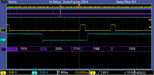
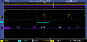
Below are signal captures from both boards: Yellow is the ALE signal, Blue is /DACK0 (meaning that memory refresh is in progress), Purple is lower 16 bits of address (as seen on the ISA bus).

IBM XT:
TEK00004.PNG

IBM PC:
TEK00005.PNG

As you can see, in both of them ALE appears in the middle of memory refresh cycle - it is not always the case, more frequently it does not appear there. Nevertheless every so often it does on both IBM PC and IBM XT.

In both IBM PC and IBM XT ALE is connected directly to the 8288 bus controller. According to the documentation, the 8288 pulses ALE every the processor transitions from T4 state to T1 state. This transition is signaled by the CPU status lines changing from S0==S1==S2==1 to anything else.

The bus arbitration and wait logic, that is used to pause the CPU during the DMA cycles monitors CPU status signals as well. In case of IBM PC, it pauses the DMA only when the current CPU bus cycle is T4 (S0==S1==S3==1). In case of IBM XT, it can be either T4, or a halt cycle (S0==S1==1, S2=don't care).

So, no major differences between PC and XT here...
 
So, no major differences between PC and XT here...
Actually, there is a huge difference in your pictures regarding to ALE signal...
Just imagine that a card uses ALE signal to latch the address. If you look at the picture of your XT, everything looks right - ALE starts just before the address bus gets the address, and goes down when the address is fully established on the bus.

But look at the PC picture now ! Yes, it works in the same way with the address 7410, but 740B (which is immediately after the refresh cycle) is completely different story. If the card uses ALE to latch the address, instead of latching 740B it will latch 4C59 - the address of the memory being refreshed...

Actually, I'm very surprised that XT picture is showing correct ALE - I can't believe it comes directly from 8288... Possibly in later XT models they added something to fix this issue...

Do you think my explanation has a sense ?
 
I see a noticeable difference between IBM XT and IBM PC at your pics. I think internal Trident's logic monitoring ALE falling edge and latch address into internal latches. Then if MEMR/MEMW/IOR/IOW signal accured TVGA chip decoding address from internal latches, not from adress bus. So, at your first picture address for TVGA decoder = 740B, seems to be ok. At your second picture address for TVGA decoder = 4C59, looks wrong. Must be 740B. But it never happens. 740B address lost. Next address for TVGA decoder = 7410.
 
Last edited:
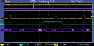
Right... It might be a bad picture ;-) I've seen ALE pulsing while DMA was outputting the address as well. The image below shows ALE and AEN (which goes high during DMA cycles) on my IBM XT board:
TEK00002.PNG

What I think, is that during the initialization TVGA chip tries to auto-detect the bus type, more specifically whether it has unlatched LA23-LA17 (as it would on 16-bit ISA), or just latched SA19-SA17, as on an XT system.

Update: Here is what IBM has to say about ALE signal in the IBM XT Technical Reference (a very similar description is also present in the IBM PC Technical Reference):
ALE (0)
Address Latch Enable: This line is provided by the 8288 Bus Controller and is used on the system board to latch valid addresses from the microprocessor. It is available to the I/O channel as an indicator of a valid microprocessor address (when used with AEN). Microprocessor addresses are latched with the falling edge of ALE.

Note the "when used with AEN" comment. The way I understand it, is that ALE should not be relied upon, and the address is not valid if AEN is inactive.

Update 2: TVGA9000i Datasheet, Table 4 shows that RMD7 is used to configure 8-bit (RMD7 pulled down) or 16-bit memory access (RMD7 open). I am not quite sure what it means, but this signal is open on my SVGA board, and on other Trident based cards that I've checked... So I am wondering if pulling that down would force the TVGA chip into 8-bit/latched addresses mode.
 
Last edited:
Hi, I just tried pulling RMD7 low with a soldered 10K resistor to ground on two different Sergey VGA cards that work OK in 16 bit bit systems. Neither card worked on a 5150 motherboard running the Anonymous Bios. BTW: Both cards still work on a 16 bit motherboard. Also, I tried a TSENG VGA card with ET4000AX in the same 8 bit system just to make sure the other parts of the setup were OK and the VGA output is working fine. My only caution is that it is REALLY hard to see and solder this pitch on a PCB, but the connections checked OK when probed with a meter.

Michael
 
According to the "IBM 5160 - Technical Reference - APR83"
http://minuszerodegrees.net/manuals.htm#IBM
page D-3
ALE goes from the pin.5 ALE of the 8288 to the 74LS373 address latches and to the B28 pin of the ISA-8 slot.
There is no another source of the ALE signal.

8288's bus Command signals are controlled by the pin.6 ^AEN and pin.15 CEN
Intel's 8288 documentation is very brief, I've used Siemens 8288 datasheet
http://pdf1.alldatasheet.com/datasheet-pdf/view/45589/SIEMENS/8288.html

As far as I understand ^AEN and CEN does not affect ALE (they control Bus Command signals only like MEMR/MEMW/IOR/IOW)

Can anyone explain extra ALE pulse during DMA cycle on the 5160 ?

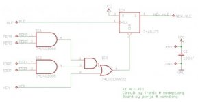
Anyway, it shoul be enought to do disable extra ALE with AND-gate: TRIDENT_ALE=ALE & ^AEN


P.S. There was a report that Trident 9000i works on the Commodore PC III (XT-class machine with chipset motherboard).
Faraday 2010 chipset may not generate extra ALE too (nobody tested).
 
According to the "IBM 5160 - Technical Reference - APR83"
http://minuszerodegrees.net/manuals.htm#IBM
page D-3
ALE goes from the pin.5 ALE of the 8288 to the 74LS373 address latches and to the B28 pin of the ISA-8 slot.
There is no another source of the ALE signal.

8288's bus Command signals are controlled by the pin.6 ^AEN and pin.15 CEN
Intel's 8288 documentation is very brief, I've used Siemens 8288 datasheet
http://pdf1.alldatasheet.com/datasheet-pdf/view/45589/SIEMENS/8288.html

As far as I understand ^AEN and CEN does not affect ALE (they control Bus Command signals only like MEMR/MEMW/IOR/IOW)

Can anyone explain extra ALE pulse during DMA cycle on the 5160 ?

Right, /AEN and CEN do not affect ALE signal. And I think that's exactly why it is being generated during DMA. As I explained above, for DMA operations, the bus arbitration logic in PC and XT inserts CPU wait cycles. Apparently, in some cases CPU's READY signal doesn't go inactive in time, and the CPU proceeds with the bus cycle, changing its status lines (S0-S2) and causing 8288 to generate ALE pulse. Normally it won't affect the operation, since the address that CPU outputs gets latched properly (it just doesn't go to ISA until the completion of DMA operation), and most of the devices don't care about ALE signal, and only care about the address then /MEMR, /MEMW, /IOR, or /IOW go low/active (or perhaps a slightly before that).

I need to find some time to hook up the logic analyzer and confirm this theory :)

Anyway, it shoul be enought to do disable extra ALE with AND-gate: TRIDENT_ALE=ALE & ^AEN
It might not work, because in this case TVGA might loose some of the memory requests.

P.S. There was a report that Trident 9000i works on the Commodore PC III (XT-class machine with chipset motherboard).
Faraday 2010 chipset may not generate extra ALE too (nobody tested).

I've actually tested it... The Micro 8088 project, I am working on now, and my previous Intel Wildcard 88 Motherboard project, are both based on Faraday FE2010A chipset, and they work fine with my TVGA9000i card. I also have a Turbo XT motherboard based on a Proton PT8010AF (which seems to be FE2010A knock-off), and it also works with TVGA.

Faraday FE2010A implements DMA the "proper" way. It doesn't use the CPU wait states for the DMA operation, instead it implements 8088's maximum mode RQ/GT arbitration protocol.

P.S. Intel's AP-67 "8086 System Design" has a lot of details on 8086/8088 bus operations. I have it, but unfortunately it is too big to be attached on this form. PM me if you want a copy.
 
Back
Top