• Please review our updated Terms and Rules here

Twentieth Anniversary Macintosh Issue

raoulduke

Experienced Member
Joined
Jan 14, 2015
Messages
356
Location
New Jersey
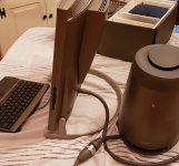
Hey, I got a pretty good deal on a Twentieth Anniversary Macintosh from the original owner. He told me he'd gotten it a few years after the release when the price came down and he and his wife had used it for at least 5 or 6 years (but maybe as many as 10) - so probably 1999-2005/2009... - and thereafter regularly powered it on roughly every 6-9 months from 2009 until it failed to power on a few weeks ago.

When I got it, it soft-powered on immediately with no problem. I booted into I think OS 7.6 and shut it down. I then soft-powered it on again with no problem. At that point I noticed the screen started to flicker shades of gray (I'm going to have trouble describing the precise problem, but people who have seen this will know what I mean, I think). I played with the connector from the machine to the subwoofer and it seemed to trigger the cycling flickering. But then when I just let it be it also flickered - where sort of columns and rose of gray, or parts of the screen or the whole screen, would randomly become gray or pop back into view and then disappear again.

I've seen this on other machines; and because of the unpredictability both of the effect itself and of the owner saying it would not power on but me having no problem, and the sort of choreography between the cycling of the effect and the booting (like it'll stay still and then when there's a burst of HD activity it'll start again), I'm pretty sure it's a capacitor problem. I'd welcome second opinions on that, though - I have at least one spare 3400c screen in storage, so it would not be difficult to swap out the screen, but I don't think that's the problem.

The bigger issue is that, assuming that's right, or maybe even anyway, assuming I want to recap my TAM... is there a capacitor list anywhere? And do I have any choice but to basically painstakingly take out the motherboard? Does anyone have any tips on that? (I'm 99% sure I'll break parts of the plastic.)
 
iFixit has a teardown guide on the TAM.

https://www.ifixit.com/Teardown/Twentieth+Anniversary+Mac+Teardown/12702

It uses the same logic board as a Power Macintosh 6500, which shared the same form factor with the Performa/Power Mac 6360 and 6400, which all use the garbage SMD electrolytics. They're pretty much guaranteed to be bad now.

I recently had to recap my Performa 6360/180 because all of the caps had failed and the machine wouldn't boot:

vnaixyuh-jpg.200466


mwltahhh-jpg.200467


I can't find a capacitor list, but they're pretty common values. I think most of mine were 47uF @ 16v with a few 100uF @ 6.3v. I used radial leaded capacitors instead of more SMDs because I find them easier to work with. All you gotta do is bend the leads out at 90 degree angles about 1/8" away from the capacitor body and snip them short so they look like back to back Ls They're easy to get a soldering under to put back on the board. I had to get creative for the ones next to the CPU though since the caps were too tall to fit. A bit of creative leg bending to lay the capacitors on their sides fixed that issue.

Something important to note is if the TAM has the 4.5V clock battery brick velcro'd to the logic board, remove it. They're prone to leaking like any other old battery type. Mine fortunately hadn't gone off, but it was 100% dead. I'd advise using a 3 x AA or AAA battery holder outside the machine and reuse the logic board connector and wires from the old battery to connect it up. You can get away with just two AA/AAA batteries if space is an issue.
 
Thanks. I saw the iFixit teardown, which is why I figured I was almost guaranteed to break a bit of plastic on something. Good point on the battery; it wasn't leaking but there's no point in leaving i there. *No visible leakage either on or from the battery.

The caps look really similar to the PB 3400... I wonder if this really was just an unfolded powerbook with a really expensive subwoofer...
 
The caps look really similar to the PB 3400... I wonder if this really was just an unfolded powerbook with a really expensive subwoofer...

No.. I just said it uses the same form factor as a PowerMac 6500.

Here is a picture of the logic board from a TAM:

YoUxHeUMLXYfUJKS.medium


Notice it looks pretty much identical to my 6400/180?
 
I think the G3 accelerators originally designed for the 6400/6500 will also work the TAM, giving it a much needed boost.
 
Notice it looks pretty much identical to my 6400/180?

It was done in the low-end desktop group as a modification to the 6x00
I was working in the same building during the development, it was pretty much a one-person (contractor) project.
The changes to sound, adding the LCD and getting it to fit in the enclosure were the main things that were done.
 
Quite a bit, especially if they included an external cache. The 603 CPU was a dog.

The 603 wasn't a bad processor, it got a bad name from the garbage machines Apple used them in, like the Performa 5200 series or 6320. The later 603e and 603ev core revisions were even better.

Both The Performa 5200 and 6320 for example used a Quadra 605 motherboard, modified to fit the 603 CPU. The bus speed remained 25 MHz, as used with the original 68040; As well as the bus width of 32 bits, despite the 603 having a 64 bit bus. As you can imagine, this machine was a dumpster fire, even though the base model 5200 had a 75 MHz 603, it was slower than a 6100/66 with the older 601 PowerPC CPU. Apple tried to offset the terrible design by bumping up the speed of the CPU, but it was so badly bottlenecked by the crippled bus that it didn't help at all and just made the machine unstable.

But it was even worse. In an attempt to balance the PowerPC's 64 bit bus, it was split into two 32 bit buses with system peripherals on each of the two buses, since Apple had a backlog of old 32 bit parts from the 680x0 era. SCSI/ADB/Comm was on one bus while the memory controller, video and IDE controller were on the other 32 bit bus. Whenever any of these devices on the different buses wanted to talk, the 603 had to stop whatever it was doing and basically act as a bus arbiter by using its registers to move data between the buses. This REALLY crippled performance and system stability, which Apple tried to solve in special system enablers and Mac OS updates.

I had a Performa 6320 about 15 years ago, it was a dog. Even with a 120 MHz 603, everything ran painfully slow. I later got a 6360, which is based on a completely different logic board design with a 160 MHz 603e and it is at least 5x faster despite the small 40 MHz clock difference. My 6500/250 is even faster still.
 
In an attempt to balance the PowerPC's 64 bit bus, it was split into two 32 bit buses with system peripherals on each of the two buses, since Apple had a backlog of old 32 bit parts from the 680x0 era. SCSI/ADB/Comm was on one bus while the memory controller, video and IDE controller were on the other 32 bit bus.

Turns out this isn't true. Not sure where this came from originally, quite possibly that infamous article on LEM, but the technical manual for those machines lists no such thing. I'm no fan of these machines either and I think they're less than they should have been but they've received probably an unjustifiably bad rap. See

https://tenfourfox.blogspot.com/2016/09/and-now-for-something-completely.html
https://www.taylordesign.net/classic-macintosh/the-mythical-road-apple/

As for the TAM, I find that the G3 yields substantial improvements, and the backside cache is a big reason why. Even with the 50MHz bus it's noticeably more sprightly with it than otherwise.
 
Turns out this isn't true. Not sure where this came from originally, quite possibly that infamous article on LEM.

It's enough to make your head ache just how cracktastic that LEM article was. The technical pronouncements within were in straight-up Dunning-Kruger territory.

Not to say those machines were great, but the bulk of their bad reputation had less to do with their system architecture (which was mediocre, but you can fairly say that about all the highest-end Macintoshes of the time) than with the software they were stuck running at introduction.
 
Turns out this isn't true. Not sure where this came from originally, quite possibly that infamous article on LEM, but the technical manual for those machines lists no such thing. I'm no fan of these machines either and I think they're less than they should have been but they've received probably an unjustifiably bad rap. See

https://tenfourfox.blogspot.com/2016/09/and-now-for-something-completely.html
https://www.taylordesign.net/classic-macintosh/the-mythical-road-apple/

I didn't read what I mentioned at LEM, it was somewhere else, but probably came from LEM originally. Daniel Taylor in the second link describes the architecture differently where bridge chips are used to cascade separate 68040 and 68030 buses to different devices, which is still an awful design, and still holds muster that Apple was trying to clear out old chip inventory. I had a 6320CD and it was awful as I said, even with OS 8.6 and 9 which supposedly fixed some issues in software didn't do the machine any favors. It died a firey death when the PSU exploded and I opted to just get rid of it since I recently got a 6360 that was better.

Though he does make an erroneous assumption that you can't split a processor data bus in half and have a working machine, which isn't true. The Sega 32x did something similar by putting two 32 bit SH2s on a 16 bit bus and ignoring the upper 16 bits of the SH2 bus to be compatible with the Genesis 68000. The Macintosh LC and LC II did the same with a 68020 and 68030 on a 16 bit bus. While the upper 16 bits of the bus weren't used in these cases, they easily could have been with different firmware and board layouts. Not that you'd want to do such a thing, it's still an awful design.
 
Though he does make an erroneous assumption that you can't split a processor data bus in half and have a working machine, which isn't true. The Sega 32x did something similar by putting two 32 bit SH2s on a 16 bit bus and ignoring the upper 16 bits of the SH2 bus to be compatible with the Genesis 68000. The Macintosh LC and LC II did the same with a 68020 and 68030 on a 16 bit bus. While the upper 16 bits of the bus weren't used in these cases, they easily could have been with different firmware and board layouts. Not that you'd want to do such a thing, it's still an awful design.

Daniel Taylor's point wasn't that you can't just "split a processor data bus in half", he goes into great detail about how it's totally possible to do it via bridge chips (and natively on the 603). His point is that the method described in that LEM article *is* impossible, IE, you can't literally just grab half the data lines from the CPU socket and route them to this half of the motherboard, route the other half somewhere else, and leave it to the CPU to just sort out. NO CPU works that way.

*Many* CPUs do have built into them the ability to operate with narrower bus sizes. The 68020/30, the 80386/80486, and many RISC CPUs (including the 603) allow an external pin (or some combination thereof) to tell the CPU that the memory/peripheral that's being accessed at the current address is only 8/16/32 bits wide instead of the maximum size, and therefore the CPU's bus unit should break longer-than-byte transfers into the appropriate chunks. (And adjust the effective addressing accordingly for each bus cycle.) There is nothing non-standard about this and it makes perfect sense to use multiple buses in a system to support peripherals with different bandwidth requirements. Until fairly recently standard PC chipsets included a highly modified/atrophied version of the original 16 bit ISA bus (AKA LCP bus) for hanging low-speed devices like multi-IO controller and keyboard chips off of; that's essentially the role that was played by the 68030 bus in the Macintosh 62/300 series Performas.

(The 68040 was actually kind of unusual for a chip of its vintage in that it did dispense with onboard bus sizing and needed a bridge chip to do it; the MC68150 was a generic off-the-shelf IC; Apple's 68040->68030 bridge ASIC essentially incorporated the same logic.)

I would mostly agree that it was probably going a bit far to put main RAM on the system controller designed for a 68040, but the CPU did have full 64 bit access to ROM and secondary cache so the hit really wasn't *that* bad. (And numbers bear that out.)
 
... although, I guess if you want to talk about ugly bus sizing you can actually bring up some limitations of Nubus, which ironically only appeared in its full form in higher-end "premium" Macintoshes. Here's an old article by Alan Cox talking about his initial port of the Linux kernel to a Macintosh II. The document contains several less than veiled swipes at Apple's hardware designs, but under the section "Mapping Ethernet Cards" is this tidbit:

Having played with the RAM behaviour a bit I discovered that the memory was mapped to every alternate 16bits in its address space. That is if you wanted to read it you had to read two bytes, skip two bytes, read two bytes etc. A bit of further experimentation revealed that the Ethernet controller registers occurred every fourth byte, that the RAM occurred every other pair of bytes and was 16bit wide and that the ethernet controller saw the 16bit wide memory as 8bit wide. Only on a Macinotsh...

The technical reason for why it would be this way is the NuBus, as implemented by Apple, has no automatic bus sizing to make it simple to interface narrower-than-32-bit peripheral chips. The CPU in a Mac always thinks a NuBus card is 32 bit and does bus cycles accordingly, so someone building a card with more humble hardware either needs to incorporate a bunch of latches and logic on their card to allow it to do 32 bit cycles the "right" way, or they need to accept the fact that a full 32 bit read will always contain some garbage bytes in it and wallpaper over the problem with the driver. A lot of Mac hardware took the latter route, which means the drivers are full of ugly hacks that are less efficient than proper hardware bus sizing would be.(*)

(* Perhaps "ugly hack" is a bit harsh, there's really not much of a problem if you're just banging away on some 8-bit registers; you just need to remember to map them at every fourth address. But it does get weird if you put something "RAM-like" on the bus and don't make it 32 bit from the Mac's point of view, like the example case of the Ethernet buffer RAM.)
 
Last edited:
IE, you can't literally just grab half the data lines from the CPU socket and route them to this half of the motherboard, route the other half somewhere else, and leave it to the CPU to just sort out. NO CPU works that way.

I wasn't agreeing with the LEM article about the "split bus and cpu figure it out", I was saying it is possible to split a data bus in half if the proper firmware and hardware existed on the board to support it. But it would be an awful design that makes no sense, unless there's some bizarre use case.

Of course splitting a CPU bus and expecting it to work without anything to tell it what's going on will not work. It'll be just reading garbage and not know what to do.

There is nothing non-standard about this and it makes perfect sense to use multiple buses in a system to support peripherals with different bandwidth requirements.

Of course it's sensible to have slower buses, but the Apple machines in question go far beyond that. Apple goes out of their way with custom ASICs to emulate two entirely different processor bus architectures and cascade them off another processor bus architecture to get slower devices working, which is a waste of time and money just to reuse some old stock of chips they had lying around. This is something I'd really only expect Apple to do.

In PC land, the ISA bus has been around since cain killed abel, and was still around when physical slots stopped being a thing, being hidden in the south bridge. It was eventually replaced by LPC, which is basically a subset of ISA at a higher clock speed. But it still is based on the x86 bus protocol.

A far simpler method for Apple would have been to put all of the low bandwidth devices on Nubus or PCI and the important things like Video and IDE directly on the 603 bus.
 
While I now have a MaxPower G3 card and more RAM in my TAM, I still only have a screen 40% of the time.

Could it really be an issue with the cable to the woofer? Are there known issues with it - maybe the solder joints?

(I don't have a buzz issue but my cable is mildly frayed at the base of the mac and this suggests moving the cable can affect the buzzing (which is I think usually alleviated by retouching the solder joints - https://www.cnet.com/news/two-follow-ups-umax-cable-glitch-twentieth-anniversary-mac-noise/ )

20191230_080852.jpg

* fray is the wrong word - the cable shielding is mildly separated fron the case-back.
 
Last edited:
I wasn't agreeing with the LEM article about the "split bus and cpu figure it out", I was saying it is possible to split a data bus in half if the proper firmware and hardware existed on the board to support it. But it would be an awful design that makes no sense, unless there's some bizarre use case.

Well, it would still depend on what you were doing. If you're just reading device registers then, sure, you can scatter them whereever you want across the full width of the data bus and write your driver so it does a full-width-word fetch and throws away all the wrong pieces. (As noted, this is essentially what you have to do on NuBus to read an 8 or 16-bit peripheral; the Mac firmware actually has a routine for reading 8-bit declaration ROM contents that figures out what "byte lane" the chip sits on, does the appropriate reads, and pieces the code back together in RAM.) But if you wanted to actually execute code directly from narrow memory you'll have to align it properly.

Of course it's sensible to have slower buses, but the Apple machines in question go far beyond that. Apple goes out of their way with custom ASICs to emulate two entirely different processor bus architectures and cascade them off another processor bus architecture to get slower devices working, which is a waste of time and money just to reuse some old stock of chips they had lying around. This is something I'd really only expect Apple to do.

Any machine more powerful than a 80286 with an ISA slot (or ISA interfaced chips on the motherboard) is doing precisely the same thing. (And ISA actually itself includes some circuitry to detect and accommodate eight bit cards designed for the 8088.) The thing to understand about why Apple stuck a 68030 "bus translator" into so many machines (and they sure did, every 68040 desktop machine they made outside of the "pure" Quadras, IE, 610,650,700,840,900 and 950 had one, as did every 68040 Powerbook *and* every PowerPC powerbook through the 1400) is the 68030 PDS was a useful stand-in for ISA; it supports dynamic bus sizing, ran at a reasonable speed (both twice as wide and fast as ISA), and was easy to interface with a whole menu of inventory chips they had lying around, both in-house ASICs and off-the-shelf chips. It makes perfect sense as glue logic for the era.

(There's no point of sticking a SCSI chip that only does 5MB/s or a serial chip that does only a tiny fraction of that directly on the native CPU bus; you'll essentially just be building its own little bus translator anyway.)

A far simpler method for Apple would have been to put all of the low bandwidth devices on Nubus or PCI and the important things like Video and IDE directly on the 603 bus.

Machines based on the 5200/6200 architecture actually debuted a month before the Power Macintosh 9500, which was the first PCI Macintosh. It would have been sort of weird for Apple particularly to go all in on incorporating the very newest and shiniest (and presumably most expensive) technology they had into the lowest end bottom-feeder Power Macs they were selling, particularly when they were still introducing new revs of the 6100/7100/8100 as "mid-range" machines.

As for Nubus, *no* Macintosh uses Nubus for motherboard interconnect, it was strictly for slots. (If you thumb through the later editions of "Designing Cards and Drivers for the Macintosh Family" and read between the lines you can almost see sitting in plain sight regret that they used a bus with so much overhead for the Mac II; they don't hold back when it comes to enumerating some of the benefits of using PDS instead.) Nubus firmware conventions are used to access devices across the spectrum of pre-PCI machines but many, if not a plurality, of the "Nubus Macs" made don't have a single Nubus ASIC in them.

Again, I will agree that those machines are chintzy and suboptimal, but that's because they are literally just a Quadra 630 with a PowerPC 603 CPU upgrade squashed onto the motherboard. (Once you go south of the "Capella" chip the architecture is 100% identical; the 630/640 computers were actually fairly decent machines for their era, mostly irrelevant gripes about IDE hard drives not being as "good" as SCSI aside.) The closest PC analog I can think of for a machine like this would be one of those rare VL-Bus Pentium computers (in that you'd have a machine with a mix of Pentium, ISA, and a 32 bit bus that's effectively 386 native), but I don't know if anyone made one of those that literally used the same motherboard chipset as a 486 machine and left the RAM on the 32 bit side of the fence. Someone may well have, I've seen some pretty sketchy motherboard chipsets before.
 
Some commodity chips (scsi,scc) were carried forward, the gate level blocks were migrated from one generation of ASICs to the next to minimize risk and changes to drivers.
Memory controllers and video were changed often, but the core I/O functions were not. The biggest dead-end I/O wise were the things added in the Q840/660AV (sound DSP
in particular) that died with the PPC cpu change.
 
(There's no point of sticking a SCSI chip that only does 5MB/s or a serial chip that does only a tiny fraction of that directly on the native CPU bus; you'll essentially just be building its own little bus translator anyway.)

This is something that never made sense to me, Apple stuck with the ancient 50 pin SCSI-1 standard until they stopped providing it on the logic board. By the mid to late 90s, newer SCSI standards had greatly improved speed, like ultra wide got up to 40 MB/s, SCSI-2 and 3 were up to 160 and 320 MB/s.

SCSI was more expensive, but it was better than potato IDE they offered on many Power Macs where PIO 3 was the fastest that was offered. I remember people with PCI power macs using PCI disk controllers because the onboard ones were so slow, especially on machines like the 9x00 where you had tons of PCI slots.
 
Back
Top