• Please review our updated Terms and Rules here

Were there ever 386 motherboards with fake cache?

DCA2's 386 board has JP3 and JP4 closed, yet he only has a 8kx8 tag piece. That contradicts earlier comments that said those jumpers control the tag size.
So the big question is why is JH1523 having issues changing the jumpers on his board. Maybe somehow the cache RAMs are defective or mislabeled?
 
DCA2's 386 board has JP3 and JP4 closed, yet he only has a 8kx8 tag piece. That contradicts earlier comments that said those jumpers control the tag size.
So the big question is why is JH1523 having issues changing the jumpers on his board.
Yes, assuming that it really is the same chipset and that the chipset features are used the same way. The blank chip with a label on it doesn't fully assure me that this is so.

Maybe somehow the cache RAMs are defective or mislabeled?
Maybe. Or it could be that the chipset is different, or an earlier version, and some features don't work the same. Hard to be sure without pulling the RAMs and testing them.
 
Maybe my (stupid?) question: when a miss occurs, how is the data exchange done between cache and DRAM? If the data has to be transferred as a block of 4k or 8k, can it be done in a single clock? If not (I guess), then does it also use the normal 32-bit bus of 386DX architecture for data exchange between cache and DRAM? It seems to me that when a cache miss occurs, the CPU has to wait for significantly long time until a block of cache has been completely refilled. Ultimately, if cache miss occurs, can we legitimately say that the whole system performance will be lower than a non-cache system in this microscopic time window? My apologize here, but I have been bothered by this question for quite a while.

In theory, a miss on a write-through cache could be handled by setting up the address and write line to the cache, and latching the data (from main memory) into the cache RAM as soon as the data setup and hold times have been met. This should allow a cache miss to be filled from main memory without stalling the CPU any more than main memory would anyway. But a cache controller that expects to fill multiple cache data words (i.e. multiple data cache entries are used for each tag line), or perform write-back caching, probably can't do this. Multiple main memory cycles would be needed to fill a miss in this case (but the hit rate may go up significantly). If it is a direct mapped write-back cache, then if the cache data is dirty it must be written to memory before the memory read to satisfy the cache miss can even begin. In theory, a smart cache design could use much wider main memory and paralleled cache data RAMs to increase the throughput to load the cache, but when the cache data RAMs are deeper rather than wider I can't imagine this is the case.
 
I installed DOS 6.22, WFW3.11 and QEMM 9.0 on this motherboard just to see how it feels/works. Pretty smooth with the 32k cache on, not so smooth when the cache isn't working. Tried a couple games, they behave as expected. I still want to try and get the whole 128k cache working if possible.
 
I installed DOS 6.22, WFW3.11 and QEMM 9.0 on this motherboard just to see how it feels/works. Pretty smooth with the 32k cache on, not so smooth when the cache isn't working. Tried a couple games, they behave as expected. I still want to try and get the whole 128k cache working if possible.

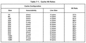
Intel states that the data in the following table may vary across software.
cache_hit_rates.jpg
 
Download a copy of Intel's 386 Hardware Reference Manual (about 13 MB as a PDF) which devotes Chapter 7 to explaining how cache works. Transfers from main memory to cache are variously 2, 4, or 8 bytes at a time depending on cache setup. It would be expected that cache fills would include the next 2 or 4 reads so most memory accesses will be from the cache. Intel's example expects a 10% slowdown if using 1kB of cache for 40% cache hit rates. Reasonable cache sizes can expect to improve memory performance by 50% or more. Theoretical worst case with software doing byte accesses that are somehow never in the cache might cut performance by about 20%*; the cache is still quite fast so misses are resolved quickly. I can't imagine any software doing that except for a possible cache benchmark torture test.

* This figure is my estimate based on timings. Please allow a large error margin for that estimate.

Thank you for clarifying that the performance drawback of cache miss does exist, and the point that the performance drawback can hardly beat the performance gain in the reality. I was ever considering to make a huge string pool sorting C program to observe the performance drawback of cache miss. But now I realized that it's not a good idea because the program code itself is sequential data, each string contains sequential chars, and I can not avoid using iterations... Indeed, it is really hard to program something useful but happens to fall into the worst case scenario.

I never realized that I can learn cache strategy from a CPU document because L2 cache management is none of CPU's business, IMO. But in fact, Intel's 386 manual contains the finest description about L2 cache I've ever seen, including update policy, write policy, coherency methods and even design examples... worth a deeper reading in future.
 
In theory, a miss on a write-through cache could be handled by setting up the address and write line to the cache, and latching the data (from main memory) into the cache RAM as soon as the data setup and hold times have been met. This should allow a cache miss to be filled from main memory without stalling the CPU any more than main memory would anyway. But a cache controller that expects to fill multiple cache data words (i.e. multiple data cache entries are used for each tag line), or perform write-back caching, probably can't do this. Multiple main memory cycles would be needed to fill a miss in this case (but the hit rate may go up significantly). If it is a direct mapped write-back cache, then if the cache data is dirty it must be written to memory before the memory read to satisfy the cache miss can even begin. In theory, a smart cache design could use much wider main memory and paralleled cache data RAMs to increase the throughput to load the cache, but when the cache data RAMs are deeper rather than wider I can't imagine this is the case.
I guess that wider (vs. deeper) cache implementation does exist if not popular, maybe the Octeck DCA was an instance. Another thought is that the CPU may not necessarily to access memory on every clock cycle. After a read or before a write, the CPU has to spend clock cycles for doing internal processing with the data on registers, giving the cache controller a short but safe chance to synchronize data between cache and main memory without holding up the CPU. But I can't find support in documents.

I also read that the cache management can be even more complicated if DMA of device I/O has to be considered... anyway, understanding the complexities and challenges does help in appreciation of the vintage hardware.
 
Runs fine on this 386.

More experiments:
- turn off L2 cache, ctcm.exe runs fine
- turn on L2 cache, ctcm.exe sometimes shows L2 cache: 128k, before stuck at "Check...5"
- turn on L2 cache, run speedsys first, then ctcm.exe can finish the job, but no cache reported

So the big question is why is JH1523 having issues changing the jumpers on his board. Maybe somehow the cache RAMs are defective or mislabeled?

Maybe the cache chips are down-graded because some blocks at higher address are found defective but the lower address blocks are still functional.
 
Last edited:
Another thought is that the CPU may not necessarily to access memory on every clock cycle. After a read or before a write, the CPU has to spend clock cycles for doing internal processing with the data on registers, giving the cache controller a short but safe chance to synchronize data between cache and main memory without holding up the CPU.

This really started to show with the 486 because of the chip's internal L1 cache. At that point the CPU only needed the memory bus for memory writes, or when a miss on the L1 cache occurred. It seems to me, from reading the functional descriptions of several chipsets, that the chipsets designed for the 486 have more cache management options, more complex cache management, etc. I even have a very late 386 board that uses a chipset that the manufacturer says was designed for the 486.
 
Maybe that's also why the L1 cache in 486DLC processor is disabled by default.

Although 486DLC is a pin-compatible replacement to 386DX, its L1 cache can only be enabled by a later BIOS that knows the corresponding chipset is able to handle more complex cache options.
 
Maybe that's also why the L1 cache in 486DLC processor is disabled by default.

Although 486DLC is a pin-compatible replacement to 386DX, its L1 cache can only be enabled by a later BIOS that knows the corresponding chipset is able to handle more complex cache options.

I have a 486dlc coming from an ebay auction; the BIOS of this motherboard has 2 options regarding cache: " enable internal cache" (which I cannot select with the current AM386DX-40) and "enable external cache"
I have great hopes for the 486DLC :)
 
I think so; but if I can enable it in BIOS, that may be moot.

BTW, if I enable the internal cache, will the motherboard cache show as L2?
 
I think so; but if I can enable it in BIOS, that may be moot.

BTW, if I enable the internal cache, will the motherboard cache show as L2?

Basically, your L1 cache is integrated in your CPU. Your L2 cache is a product of your motherboard and can be toggled on/off via your BIOS setting. For optimum performance you would want the L2 cache on.
 
I know that, but right now my L2 shows up and acts as L1. :)

How did you determine that? Are you saying that overall, your system is running slower with the L2 enabled through the BIOS? BTW, the 486 is the only CPU that I know of (there may be others - Cyrix comes to mind) that you can disable the L1 by mean of external software; i.e., a cache on/off executable. In my experience, and generally speaking, the only time you would need to disable a cache is if some 8-bit program is stubbing its toe.
 
No, I'm saying that the motherboard cache which right now is the only cache in this system, is detected by test programs and labeled as L1, not L2. Which makes sense since the CPU has no internal cache (AM386DX-40)
 
There is indeed software to enable the cache on the DLC. However, this software was more commonly used on boards that did not properly support the DLC. However, I have not had great luck with enabling the L1 cache in the BIOS on boards that supposedly support the CPU either. I found it caused cache coherency issues with my DMA SCSI cards. I am sometimes able to bypass this problem by disabling the L1 cache in the BIOS, setting some CPU registers and then enabling the cache through the software utility. So you can try the BIOS enable, but it may or may not work depending on your hardware configuration, in which case you'll have to try the software util.
Also, there are at least two different methods for maintaining cache coherency on DLC motherboards. I think hidden refresh is the most common, because it requires less modification to the motherboard. However, there is a performance penalty. The other method involved wiring up the #flush pin on the cyrix CPU to the chipset. I have yet to see a board that uses that method, but I suspect it is more compatible with my SCSI cards.
 
I have great hopes for the 486DLC :)

I spent a little time going over the specs on the Cyrix 486DLC with its on-board L1 cache, and I believe you will eventually see both caches (L1/L2) providing your mobo's BIOS can support it. The 486DLC wasn't around that long, as I remember going from a 386SX-20 to a 486 and then on to Pentium in relatively short period of time. I'm really interested in how this shakes out for you as I now have a 386 in my collection, but haven't had the opportunity to crack it open yet. BTW, it's a desktop and weighs a ton. Good luck.
 
I bought a 386DX40 in 1997 for $10 at a swap meet that had fake cache - if I remember right it had the same form factor as the ones in your picture. It had cache chips soldered to the board, but reported no L2 cache when booted. It was an absolute slug of a thing and I kept the RAM and threw it out not long after buying it.
 
Back
Top