• Please review our updated Terms and Rules here

XT-FDC project level of interest

Hi
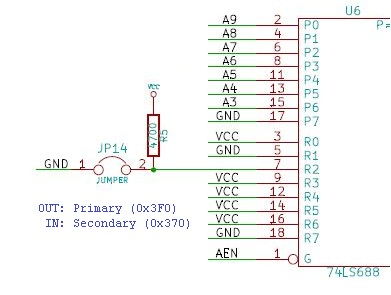
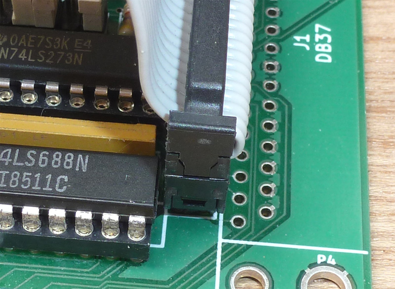
What I am trying to find out is whether the XT-FDC prototype has stabilized enough to start making the changes to the "final" board. Sometimes problems surface late in build and test especially during the software development (BIOS).

There is a preliminary change list already but I suspect there is more to be found as testing progresses. Once the board goes final we are stuck with it and any changes require cuts and jumpers/dead-bugs for each PCB.

There is plenty of time though. No hurry, I'd rather have thorough build and test than be in a rush and miss something important.

Thanks and have a nice day!

Andrew Lynch
 
Hi

Well, I know that build and test is not yet complete but I had some spare time today and started updating the XT-FDC schematic and PCB layout.

The VCF wiki has the change list here

http://www.vintage-computer.com/vcforum/showwiki.php?title=XT-FDC+Rev1

1. Fix the bit A7 decoding for the I/O port.

status: fixed

2. I can give you exact positions relative to the ISA edge connector; will that do for the external connector? (I need a reference point)

status: need help. Where exactly does the external connector go? Would you give me a relative location from where it is now? (move it right 20 mils)

3. The second internal drive connector P2 needs to be moved a bit away from the external (DC37) position--otherwise, there's too little clearance if both are installed.

status: fixed

4. The 50-pin 8" header needs to be moved over as well (too close to the bracket side of the board.

status: fixed

5. Add some space between the crystal/10 pF caps (C12/13) and the PLCC pads so that there's clearance for them after a PLCC socket is installed.

status: fixed. changed all capacitors to the larger C2 footprint to ease compatibility and parts fit issues.

6. Put some distance between JP11 and P18.

status: fixed

7. Drop the DP8473 and associated components.

status: not fixed. It seems to me the DP8473 is worth keeping as a DNP section it is basically "free"

8. Adding some 74LS07 drivers (do you want to add receivers) might give a little protection.

status: need help. What signals should be buffered? Input and output? Internal and external connectors or just external? The outputs would need pull up resistors and it adds to the parts count. I think we should discuss this more. It is doable but is it worthwhile?

9. Very minor, but I hate to see Vcc on a jumper pin--too much possibility for mayhem. Can K9 be made a simple 2-pin affair that simply grounds a pulled-up pin?

status: fixed


I posted the schematic and PCB layout files on the N8VEM wiki here

http://n8vem-sbc.pbworks.com/w/browse/#view=ViewFolder&param=XT-FDC


I reviewed the last several weeks of posts in this thread and tried to capture all the changes. For instance, I added little triangles to the connectors to identify pin 1 and generally rearranged things to help improve the layout.

Please closely review the schematic and PCB layout and send me your comments, changes, corrections, etc. Thanks and have a happy holidays!

Andrew Lynch

PS, does anyone anticipate any major changes to the design from the rest of build and test? It seems we've hit all the high points already and most everything has gone through some level of "shake down". Thoughts?
 
Please closely review the schematic and PCB layout and send me your comments, changes, corrections, etc.
1. Schematic: On U6, you've accidentally changed pin 5 from VCC to GND. It should have been pin 16 that was changed.

2. Layout: Pin 1 indication is great. Is it possible to make the triangle bigger for the cable connectors P18 and P6? I can just see it getting covered when a shrouded header (as shown for P18/P6 [here]) is soldered in place.

3. Layout: I presume that pin 1 indication on 2-pin jumpers, such as JP6, is done only to support possible diagnostic work. Otherwise, I can't see any point.

4. Layout: Re transistor Q1. Options are 2N2222 or 2N3904. People will probably source the TO-92 packaged versions of them. As shown right side if the photo [here], the 2N2222 is orientated differently to the 2N3904. Perhaps remove the Q1 ouline, or change the outline to a circle, to greatly reduce the possibility of someone inserting a transistor in the wrong orientation (people would be forced to seek orientation guidance elsewhere).

5. Layout: To avoid jumper confusion, is it possible for the JP6/JP7/JP9 labels to be moved from the 12 o'clock position to the 9 o'clock position?

6. Schematic: A suggestion. Change of JP14 comment to:

jp14_suggested_comment.jpg

Thanks!

1. D'oh! Good catch! My bad. Fixed.
2. Fixed, added larger triangles. Hopefully that should be enough to poke through under the shrouds
3. Yes, pin 1 is only meaningful on larger jumper sets. Oh well the little triangles don't hurt anything.
4. Yes, I specified 2N3904 NPN which uses the "TO92-invert" footprint. Agree that 2N2222 uses "TO92" and since they are not consistent it has caused me no end of grief on other boards. Lets just stick with 2N3904 and if builders want to install a 2N2222 they can do it against the footprint. I am sort of stuck with what footprints KiCAD has for transistors.
5. Fixed.
6. Fixed.

I will upload revised schematic and PCB layout files. Please review to ensure these are accurate.

Thanks and have a happy holidays!

Andrew Lynch

PS What to do about the external floppy connector? It would be nice if we could move the whole footprint over so to free up some more room for traces. I have no idea exactly where it is supposed to be.

PPS so if I read the previous posts correctly, the XT-FDC works with Sergey's BIOS code. Does that mean the BIOS code is done? Where are we with the BIOS? I seem to be missing something.
 
Last edited:
Per Chuck's November 9th post, the hardware is already in place - the TG43 pin (pin 2 of P6) being connected to the 8477, all ready to be software controlled as required.

I don't anticipate much use of the 8" interface by others. Myself, I use an FDADAP.

Any way you look at it, if you want to put TG43 under program control, it's going to be custom code. You can either do it through the 8477, or you can use an external latch pin. I don't imagine either really happening--most of the software for 8" is already in place and most assumes that TG43 is handled automatically, via FDADAP or some other mechanism (e.g. on-drive circuitry).
 
lynchaj said:
8. Adding some 74LS07 drivers (do you want to add receivers) might give a little protection

status: need help. What signals should be buffered? Input and output? Internal and external connectors or just external? The outputs would need pull up resistors and it adds to the parts count. I think we should discuss this more. It is doable but is it worthwhile?

I'm less concerned about receivers than transmiters. You're probably best off doing both internal and external, as most important ones are shared anyway. I'm mostly interested in avoiding damage to the FDC from overshoot on too-long cables and the issue of an extra unintended 150 ohm terminator on older drives causing the 8477 to sink too much current. Better to pop a cheap 7407 than a rare LSI chip.
 
PPS so if I read the previous posts correctly, the XT-FDC works with Sergey's BIOS code. Does that mean the BIOS code is done? Where are we with the BIOS? I seem to be missing something.

My current code is a straight forward copy of floppy code from my BIOS. It supports only 2 drives on the primary controller address with IRQ6/DRQ1. Adding 4 drives support, secondary controller address, configurable IRQ/DRQ will require considerable rework.

Also currently it doesn't have an utility to configure drive types (hex editor is required). I have plans to implement a built-in configuration utility that will store configuration directly to the BIOS extension EEPROM. Hopefully I'll get to it later this week.
 
PS What to do about the external floppy connector? It would be nice if we could move the whole footprint over so to free up some more room for traces. I have no idea exactly where it is supposed to be.
I'm sure that is in regards to Chuck's suggested change of, "The second internal drive connector P2 needs to be moved a bit away from the external (DC37) position--otherwise, there's too little clearance if both are installed."

Chuck is yet to comment on the distance, but the photo below gives you a good idea of the sitation, and may lead you to come up with your own adjustment.

xtfdc_p2_j1_gap.jpg
 
I don't imagine either really happening--most of the software for 8" is already in place and most assumes that TG43 is handled automatically, via FDADAP or some other mechanism (e.g. on-drive circuitry).
Yes. I had earlier written the following to Andrew:

We may end up telling people, "Here are the known limitations, and here are some jumper settings to use for some common 8" drives. Outside of that, if there's a problem and you are sure it's not the XT-FDC [faulty] and not due to jumper settings on the drive, etc., then maybe an FDADAP board will work for your scenario."
 
Hi
Yes, I see the secondary internal connector is too tight with the external connector. I shifted the whole circuitry over to the left 100 mils so there is 50 mils on either side of the secondary internal connector now.

Still, it would be better if we could move the external connector over to the right a bit.

Thanks and have a happy holidays!

Andrew Lynch
 
Hi

I updated the XT-FDC schematic and PCB layout to buffer the outputs from the FDCs to the connectors.

All of the inputs and outputs are now buffered. However the PCB is full of parts and it is going to be difficult to trace route this board and no new components can be added.

http://n8vem-sbc.pbworks.com/w/browse/#view=ViewFolder&param=XT-FDC

Please review the schematic and PCB layout and post your comments, thoughts, and/or questions.

Thanks and have a happy holidays!

Andrew Lynch
 
Last edited:
DRQ2 it is :)

BTW is there any standard for IRQ/DRQ for the secondary controller, or they were just picked arbitrarily from the available lines?

The most common scheme was to share DRQ2/IRQ6 with the primary controller, since these can be shared via port 3x2 control.
 
I'm confused about adding the buffers. Whatever you put there must have an OC sink capacity of > 40 mA. More if there's improper termination on the bus. Are you not worried you'll be going from a situation where you might blow up a rare ASIC to you'll routinely burn out buffers?

It's probably an issue only for older drives. I suspect newer drives have stronger pulls on the far side. But at the very least I would spec a specific part or specific part requirement to builders.
 
I don't think that you'd routinely burn out buffers, even using a 7407 (7438 is the traditional driver for this kind of interface). If the 40ma rating of a 7407 is a problem, I suspect that a 75451-type driver might do. But preserving the hard-to-get PC8477 is a reasonable measure, I think.

An addendum on the DRQ2/IRQ6 issue. There are a few systems with integrated FDCs that cannot relinquish those resources (a Tandy 1000 IIRC, is one of those) via the 3F2 "enable" bits. That's a reason for alternatives.
 
NXP has a 74F07 in stock at most places in DIP that has a rated sink capacity of 64mA per pin. Though it doesn't state what the common current limit is. It should be fine, but there are many '07s (and '38s) from different sources that spec much less.
 
Hi
Last night I got the XT-FDC PCB to trace route. It is cleaning up in the optimizer now and will probably be there for a while. In the mean time we can finish up build and test and hopefully shake out any remaining problems. Later tonight I will post the updated schematic and PCB layout for review.

I don't know when it will be ready for a PCB manufacturing order but I am thinking the first batch will be a small one like 10 boards or so. If those work out OK then open it up to a broader audience.

Thanks and have a happy holidays!

Andrew Lynch

PS, the only thing left on the "fix list" AFAIK is doing something with the external connector. It hasn't moved any so if someone would please send me some measurements I could make adjustments as needed.
 
Hi

I estimate it will cost $240 for 20 XT-FDC PCBs with shipping and tooling fees based on similar XT-IDE V2 orders.

Is there sufficient interest in an early production test run of PCBs to get a small batch?

It seems build and test and/or BIOS development is over as best I can tell.

I am thinking this would be just like the initial XT-IDE V2 test batch for production boards.

If there are any further problems we can roll the fixes into an update.

Since the small batch PCBs are a bit more expensive and there is no margin on these I am thinking $12 each plus $3 shipping in the US or $6 elsewhere in advance via PayPal.

I'd make the order when I get to 20 "firm" pre-orders to mitigate my risk of unsold boards.

Probably should be the more experienced builders for the first run boards in case there are more problems but the prototype came through build and test relatively clean.

Thoughts? Ideas? Comments? Please let's discuss.

Thanks and have a happy holidays!

Andrew Lynch

PS, due to some recent "issues" I've been having with shipping PCBs, I am adding delivery confirmation (tracking) option. It increases everyone's shipping costs by a $1 but it is worth the peace of mind when dealing with the increasingly unreliable USPS.
 
Last edited:
Back
Top