• Please review our updated Terms and Rules here

Project to create an ATX 80286 mainboard based on the IBM 5170

A photo of my most recent mod to the DS12885 to make it compatible with a mainboard designed for the MC146818.

I have tested this method for several hours of off time and it's keeping the settings fine, which is starting to look completely "PC worthy" stable.
 

Attachments

  • DS12885 to MC146818 mainboard mod.jpg
    DS12885 to MC146818 mainboard mod.jpg
    280.3 KB · Views: 11
Last edited:
While checking and documenting the ARC circuits I have found some good and bad things.

Apparently there is an open input pin on the memory databus directional control logic, I have checked the pin (after removing the IC) with 20 megaohm range measurements, and visually inspected the pad with a microscope and strong lighting behind the PCB. It is in fact an open input on a 74F logic family AND gate. Both mainboards have the same layout which is missing that input connection. The pin is right next to a VCC pin so maybe that's helping it not to not having been an issue. Though this could be a possible reason for my first mainboard to suddenly start failing without any apparent cause.

The ARC has three PAL chips, the third is dedicated to generate the CAS signals for 4 banks of RAM taking the total memory to 1MB. Though it's interesting, but since I am going to use SRAM, less important for my project.
 
I have done some testing because of the open pin 13 on U55D on the ARC mainboard.
Apparently the 74F08 leaves an open input at a certain voltage level, which - in my case - it interprets as a logic 1.
So it appears not to be a problem on my ARC X286 Model 12 mainboard.
However, I can't assume that there are no actual sporadic problems possible to arise from this.
I have tested with a 1k pull up resistor however this appears to have undesired effects on stability.
So I have tested by soldering pin 13 to VCC(pin 14) directly and tested with this option, the mainboard seems to be stable after this change. I have left the PC running for a while and I could not detect any hot chips.
As mentioned before, I have checked U55 pin 13 on the PCB optically with strong backlight after completely desoldering U55 since it's a 4 layer PCB, and I cannot detect any resistance up to 20 Mega Ohm to VCC and GND.
I have measured agains all pins on the mainboard and found no connections either.

If anyone is having problems with this ARC X286 Model 12 mainboard, and wants to have a check/try, at your own risk(!) you could do the same things as me, checking if there is indeed no connection after removing U55, and then doing the same modification. It's your own decision and risk if you do so, so use your own judgement and experience with your mainboard if anyone finds this information.

Especially after my experiences with the first ARC X286 Model 12 mainboard, where it suddenly started to become unstable at power on, these symptoms I have seen in my case:
- inconsistent initialization of VGA display, needs resets to initialize the display correctly
- when testing with MR BIOS, erratic detection of IDE, FDD and COM/LPT ports at power on, which then needs a reset for proper detection and setting the floppy drive options correctly again in the MR BIOS setup.
The gate in question, U55D, is involved in passing through the /CS signal for the BIOS.
Apparently the designers had some intention to add another signal in the logic, or they intended to introduce a small delay of the /CS signal to arrive into the databus direction logic. I have seen other areas on the PCB where they soldered some inputs to GND on the bottom of the PCB so this was not carefully checked at the design phase.

Definately the ARC mainboard is less stable than the 5170, however it does have the advantage of higher clock speed and more DRAM onboard. While testing the ARC more and sorting out the entire schematic, I will attempt to fix problems as I come across possible causes in the logic. After I have the full schematic I can also have a closer look at my first ARC PCB which is of a much higher manufacturing quality, though unfortunately it does contain many wires on the bottom. If I can't be satisfied with the final stability outcome of the ARC, I will not be using any circuits from this mainboard as a possible reference or inspiration for the new project schematic design.
 
Last edited:
I have created a blog page about this project on my website, I will also post additional info and status updates about my project at that page.

Recently, I have also started my actual design work for the mainboard for this project.

I am drafting the memory map and I am also keeping a document which lists certain symptoms and their possible causes which may aid me later when I am testing and debugging the new mainboard.

I will directly implement 128kb of UMB RAM in segments D and E in the first 1MB area which can be loaded in DOS by UMB device drivers, and I will include a space for XT-IDE(version for AT interface) and possible other expansion ROM code, totalling 32KB at C8000-D0000. I will include a normal 8 bit 27256 EPROM socket for this purpose. So there will be the two regular F segment BIOS EPROMS which support two BIOS versions with a selection jumper, and the third EPROM for option ROM code.

I plan to support both the MC146818 and DS12885 RTCs with a few jumpers and optional resistors, where the DS12885 will be able to function in the same typical "AT" way as the MC146818 in the method I have determined previously and mentioned in this thread. 5V Standby of the ATX PSU will be used to maintain the clock and CMOS settings at power off state, and only when the PSU is left unplugged from mains the external battery will be used to keep the settings and time. I plan to feature a battery connector in the IO shield area to keep the RTC battery completely outside of the PC case.

Kind regards,

Rodney
 
For this 286 project I will be changing mouse support.
My old serial mouse is really not a great device to use so I started to look around for some modern projects which offer a better mouse control than the serial mouse.

I found the right solution, a USB to serial mouse adapter done by CalamityLime, GitHub user LimeProgramming. Adams advanced project offers the connection of a modern USB mouse, including a wireless one to a vintage PC.

I recreated his project in a simplified way to reduce the circuits for the smallest footprint on my mainboard, it was up and running in about an hour and I proceeded to test the interface with my ARC 286 mainboard. I was really impressed with the improved level of control using my regular wireless PC mouse on a 286. It feels the same as controlling windows on a modern PC. There are some most relevant jumper options to easily change the mouse travel speed which I did, and it's even possible to log into a serial programming interface via serial terminal to change even more advanced settings, though I had no need to look at this yet. His solution just works perfectly by default in my opinion and I only regret not trying it sooner. My experimental version is now already a definate keeper!

I fully realise that the RP2040 used is far more powerful than a 286 itself, but I really don't mind this fact at all, the most important thing to me is that it improves my mouse control greatly and will be very helpful to have a much more smooth mouse experience using my new mainboard design. I will probably make the COM port used in standard TTL voltages and directly allow 5V communications of the RP2040 interface with some input voltage divider resistors for 3.3V input adaptation, so I will omit the 12V level shifting logic on the mouse input COM port. I will feature a USB connector for the USB mouse(receiver) in the I/O shield area.

I really can highly recommend this USB to serial mouse adapter project featured on GitHub especially for hobbyist enthousiasts who want to use a mouse and found the classic serial mice not too great when using them, especially since there is a much more advanced alternative available:


In terms of the keyboard, I am happy with the excellent quality of my Cherry G80-1000, and all PS/2 keyboards I tried worked fine too with a small PS/2 to DIN adapter cable.

I had a brief look at adapting the AT keyboard controller to function in PS/2 mode, adding support for a PS/2 mouse to be used, however it's also not really necessary now so less of a priority in the project. I will see of it could be an easy option to add, just for completeness of my project and proof of concept since many newer keyboard controllers do have this optional capability anyway. I will probably add a IRQ12 jumper for this option if it is possible to support this function from the BIOS. I will post more about that later.

Kind regards,

Rodney
 

Attachments

  • Img_2844s.jpg
    Img_2844s.jpg
    557.8 KB · Views: 8
I have been working hard on my 286 mainboard design using the 5170 as a starting point.

So far I have finished the new memory subsystem. It will feature 640kb base memory, 128kb UMB memory switchable by jumpers to load DOS drivers high, and 4MB of XMS memory. I will include a separate 32kb EPROM for option ROM code from 0C8000 - 0CFFFF.

Before I commit to some PCBs, I am now focussing on the PAL chips first to avoid needing those in my prototype.
I have made an approximation schematic of U130 based on several sources of information and various manuals which explain the operation. I attached the equivalent schematic of my last revision for U130. It will be further revised once I have the entire system schematic in a complete form where I will further reduce and change everything for a final version. For the moment I am focussing first on completeness and accuracy of the logic, and paying less attention to which gates I use where etc., which will come later. So what I am sharing at this stage is just intended to show the equivalent logic, and by no means definitive.
U130 was relatively simple to estimate, I will do further probing of the IC in a test circuit later to confirm some things.

In the mean time, I have built a logic testing circuit which allows me to test combinations of signals logically according to operation and function in the 5170, which will save time compared to brute force analysis which I believe has some shortcomings anyway. I prefer the new approach I am using now by analyzing the schematic, and observing the actual operation of the PAL itself in a TTL test circuit.

I attached a photo of my test method. Basically only TTL ICs are touching the inputs and outputs of the PAL, and on the other side of that logic I have placed switches and LEDs to change the input states and monitor the output responses by the PAL.

I am working on the PAL U87 at the moment which is more complex than U130. The PAL has 13 inputs and 5 outputs.
The first output I analysed is DATA_CONV. After a lot of testing I believe I have a complete schematic for DATA_CONV. There are several conditional signals included in the path to the output. DATA_CONV determines whether there will be an 8 bit data bus conversion to and from 16 bit. So the signal switches conversion on and off together with various other circuits.

I have attached the circuit for DATA_CONV here as well.

I will proceed to test further to accumulate all the logic inside U87. I may try to build an equivalent PCB to plug it into the socket of U87, it depends on the total size of the logic which is already quite a lot for the first output pin.

kind regards,

Rodney
 

Attachments

  • Test circuit PAL U87.jpg
    Test circuit PAL U87.jpg
    235.1 KB · Views: 10
  • U130_version_002.png
    U130_version_002.png
    19.9 KB · Views: 10
  • DATA_CONV.png
    DATA_CONV.png
    13.4 KB · Views: 9
Hi Alex,

Nice to see your reply.
I totally agree, the chip count is growing still.

From this we can clearly see that IBM had good reason to use the PALs and it was definately a consideration from a circuit complexity and PCB size perspective.
This is mainly due to the complexity of the databus conversion mechanism which needs to be adjusted for every possible combination of operation modes.

Without the PALs the 5170 mainboards could never have fit their PCB space in the 5170 case.
Which is telling to show that they still intended the standard to stay open at that moment but the PALs were simply a necessity.
Though they were not releasing the PAL source code either.

I won't be needing the PCB surface for the DRAM, refresh and parity circuits and I am reducing 4 EPROM sockets to 3.
So I will gain some PCB space on the full size ATX form factor.
Also I won't need 8 ISA slots, only 7.
I could fit the CPU and NPU on an exchangable module.

However, I am now wondering about after I have implemented all the PAL logic in TTL chips, if I can have any space for the PC interfaces, which is my goal after all, to make an integrated 286 mainboard which offers much functionality onboard. So in the same spirit as my XT design. Which only plugs in a VGA and sound card and you're done including onboard LAN and SCSI.
I aim to do the AT design in the same manner.
I don't see much point of doing the mainboard otherwise, there are a few things which really must become a part of the project to make it worth my while to manufacture and assemble the PCB.
If I still need many cards that is not my design goal.

I am considering my option to assemble a new PAL chip after all, since the circuit of U87 is proving to be extensive.
I could analyse the total logic in U87 after completion, probably this can provide some reductions but those will be only minor I believe.
Either way I choose to go, the programmed logic, if any, will be open source as deduced from the PAL operation.

I really don't like PALs because using programmable logic is somewhat restrictive.
On the other hand, I don't think many people will want to build my project so maybe I should be open for this and other changes anyway.
If I use programmable logic, it kind of defeats the purpose of using many TTL components next to the PALs or whatever it will be.
I wanted to keep the design PAL-free however now it's a consideration of at what component cost that can happen and what onboard devices would be lost due to space limitations.

Some compromises will need to be made, I need to think more carefully about this matter later.
Perhaps using some CPLD would be preferable otherwise it will become a mainboard-only PCB, no integration.
Or even a kind of PROM decoder or something.
I had hoped the PALs would be not too complex, but of course, they are turning out to be.

I just discovered another logic term which needs to be included with DATA_CONV.
So here is an updated DATA_CONV schematic.
I am now working on the 245 enables which are a part of the conversion process.

Kind regards,

Rodney
 

Attachments

  • DATA_CONV_latest 29-12-2023.png
    DATA_CONV_latest 29-12-2023.png
    15.3 KB · Views: 5
Last edited:
I have done a lot of testing today and made a best effort to try to evaluate all combinations of inputs and drafted the first version of the entire U87 now.
The result is in my attachment, a first revision. Despite my hard work, there is always a chance I may have overlooked some signal.
I didn't observe any latching action, as far as that could possibly be seen of course.
The logic in the schematic is 100% conform with what I observed in the signals, and has been cross checked with the PAL after creating the schematics.

The switches had some slight bounce which I tried to catch with some 470pF capacitors, which already made a big improvement.
Just occasionally I would get some double action or needed to press a button once again, but not too bad and quite reasonable this setup.

I will try to do some simulations and perhaps see if I can generate some verilog or PAL assembly using some kind of tools to return the entire design back into a PAL.
I will search my parts supply if I can find some obsolete PAL somewhere and try to erase and program one.
That would be the most straightforward method of testing the validity and completeness of the PAL logic.

First I need to research about PALs because I don't have any experience other than once converting some PAL source back into normal logic.
If anyone has some useful tips for me I would appreciate the help.
Like which tools and where to get a helpful software.
I found an online simulator of logic which can generate verilog code.
So I may attempt to use it but the user interface is somewhat difficult to use for correcting the circuit once a connection snapped to the wrong spot.

Kind regards,

Rodney
 

Attachments

  • U87_COMPLETE_V1.png
    U87_COMPLETE_V1.png
    33.7 KB · Views: 4
I will search my parts supply if I can find some obsolete PAL somewhere and try to erase and program one.

PALs are not reprogrammable. They're like PROMs, IE, they have literal tungsten fuses in them and once they're blown they're blown.

GALs on the other hand *are* reprogrammable. The modern (still manufactured) ATF16v8 and ATF22v10 CMOS SPLDs can emulate and are mostly drop-in replacements for most obsolete 20 and 24 pin PALs, both the combinatorial-only and registered flavors. (As are the discontinued but *very* readily available Lattice GAL16v8, 20v8, and 22v10; I've bought obviously used ones of these off AliExpress and I haven't had much trouble erasing and reprogramming them.) Both the Atmel/Microchip and Lattice GAL families are supported by the cheap TL866-style programmers you can nab off Amazon or whatever for cheap, so it's pretty easy to use them for amateur projects.

If anyone has some useful tips for me I would appreciate the help.

I did a YouTube video about the basics of using GALs for a video generation project a couple years ago, but I'm hesitant to post it here because it's an hour long, rambly and unscripted, and the auto quality is horrendous. Here's a ten cent summary:

  1. GALs aren't usually programmed in Verilog, but I guess doing a quick search on the subject it looks like it *is* a thing people do. If that's what you want to do, well, google "Verilog GAL" and go to town.
  2. Usually people talk about using a language called CUPL to program them. Microchip provides an IDE called WinCUPL for free that supports GALs and their older/smaller CPLDs. It's old, cranky software that runs better under WINE than it does modern versions of Windows and even then is still crashy if you give it invalid inputs, but if you're willing to get over the learning curve it has useful tools like a simulator that will let you verify your designs without burning them.
  3. If CUPL is overkill or WinCUPL makes you cry trying to get it to work GALasm is an open source implementation of an older hardware description language called PALASM. If you're looking through a manual from the 1980's that has the equations for a PAL in it it's probably going to be in PALASM format, and translating them to GALasm is trivial. (GALasm has a couple small syntax differences in how it denotes things like registered outputs, but it's mostly just "use a different letter" type things, not a big deal.)
Both GALasm and WinCUPL produce .pld files that can be used directly by the TL866 programmer software to program a GAL, and the wonderful thing about GALs is if you screw up your program you can pull the GAL back out of your test board and reprogram it, so unless you *really* foul up you can actually fix bugs even after you've baked a PCB with less hacking and patching than the same with discrete logic. The learning curve is kind of steep if you've never used programmable logic before (I hadn't), but once you get it down you'll be amazed at how much you can do with one chip. (The biggest limitation is mostly just that there's only a single CLOCK input for registered mode, it'd be cool if you could arbitrarily assign inputs as additional clock pins, but some non-linear thinking can kind of get around that.)

For laughs here's GALasm code for a 6502 memory decoder I wrote. It's only combinatorial logic but it looks like the PAL you were talking about here is also only that. It'll give you an idea what the logic looks like. For this sort of thing WinCUPL is definitely overkill, although it does have some nice features like a macro system that lets you express things like memory addresses as hex numbers it automatically translates to the necessary input pin bit patterns.

Code:
GAL20V8  ; memory decoder
MEMSELEC ; done

NC     PHI    A7    A15  A14   A13   A12    A11    A10    A9     A8    GND
NC     CPURW  NC    NC   WRITE READ  IOSEL  RAMSEL ROMSEL NC     RESET VCC


/ROMSEL = /RESET
    + A15 * A14 * /A13 * RESET
    + A15 * /A14 * A13 * RESET
    + A15 * A14 * A13 * /A12 * /A11 * RESET
    + A15 * A14 * A13 * /A12 * A11 * /A10 * /A9 * A8 * RESET
    + A15 * A14 * A13 * A12 * RESET

/IOSEL = A15 * A14 * A13 * /A12 * A11 * /A10 * /A9 * /A8 * RESET

/RAMSEL = /A15 * RESET
    + A15 * /A14 * /A13 * RESET

/READ = CPURW * PHI
      + /PHI

/WRITE = /CPURW * PHI


DESCRIPTION

; Decoder for 6502 computer memory space
; Inputs:
; A7-A15 Top 9 address lines
; CPURW  6502 R/W line
; PHI    HIGH = CPU, LOW = Video
; Outputs:
; ROMSEL = 20K from B000-FFFF minus IOSEL
; IOSEL  = 256 bytes at E800
; RAMSEL = 44k from 0000 to AFFF
;          128 bytes at E880
 
PALs are not reprogrammable. They're like PROMs, IE, they have literal tungsten fuses in them and once they're blown they're blown.
Hi Eudimorphodon,

Thanks for your elaborate explanation, I appreciate the effort you made and the time you took to help me by pointing to some important aspects involved since this is new to me. This saves me a lot of time to read these things from you since you already have experience, so thanks for the friendly help! If you have any other things you want to share, it's welcome to share it here if you have time.

I made the error indeed to assume that I can erase PAL chips. So another thing learned now.
Which explains the type differences and those types I could not find in the programmable type list in my device.

Yesterday I jumped into the rabbithole of programmable logic, but I am used to that because my whole PC projects are all big rabbit holes where you have to jump in and stay in. I spent some time searching methods and finally settled on using WinCupl which still works in Windows 10. Or else I have some older PCs available to use if needed. It is indeed cranky as you say but I don't mind that, at least it can provide a solution that works and it is GUI-based.

I experimented a little with the syntax in WinCupl by first only defining the pins and compiling an "empty" chip, where I picked G16V8A in the "device" field.

Compiling an empty chip was finally successful so I proceeded to write some simple equations, first one, then another.
Each time I did a compile action until there were no errors in the syntax.

I assume the syntax of equations in WinCupl is much like doing calculations where you first do the multiplications, then the sums etc. So AND goes before OR. However I was not sure so I used brackets to include circuits in the formula just to be sure.
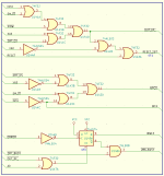
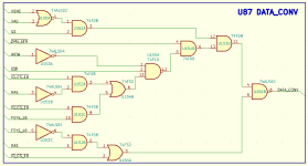
By the time I defined DATA_CONV it did get a little complicated so I finally started to use colours for the different areas to keep an overview. I was already sure I was over complicating it for myself but I continued until I at least got the whole equation defined in one line. Next time I get this kind of situation I will redraw the schematic in the form of AND terms which I can then get a better overview and I could try it without brackets later. Compiling my bracket version went fine so I proceeded to generate a .jed "fuse map" file which needs a few options to be enabled in WinCupl as I found out. After getting the .jed file it was the next step to proceed with the programmer.

I use an old Galep-III programmer which lists a number of known devices from manufacturer categories including some PAL types. Possibly certain special newer PAL type chips are erasable, I suspect this because the device lists these to be able to be erased. ICs you can erase are always bold letters in the list and allow to be selected as a "to be programmed" device. Though lets forget it since I don't have any those bold type ICs which would more closely match the PAL16L8 used in that time period. I would prefer some slower device to better match with what IBM did in the 5170, but I am willing to experiment. I do prefer devices which are more programmer friendly if possible, like the GAL.

After trying to erase some PAL chips which failed because they were OTP chips, I moved on to some GAL chips which I found later on some obsolete PCBs. I tried a Lattice GAL16V8A which programmed fine and was listed exactly with that type in the software. Ok, progress!

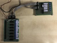
After programming the chip I plugged it into my test board which lit up some outputs with LEDs which looked promising.
I toggled a few buttons on the inputs which resulted in some familiar responses from the GAL.

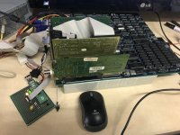
After which I built up my 5170 mainboard on my table and plugged in the programmed GAL.
Unfortunately, which I expected would be a possibility but let's try anyway, no POST and no image on the VGA and no beeps either.

So on the hardware level the 5170 is not getting through to any level of being able to function yet with the equations I have assembed so far. So it's back to evaluate everything further, but it is still a level of progress now because I have a path to the GAL device from a situation of using equations. Indeed, if one GAL can replace more than 10 normal ICs that does have possibilities in certain large volume TTL logic systems.

Thanks a lot for the explanations, I will look at the IBM PAL again in the circuit.

As the IBM schematic lists a "HAL16L8" which I think is a kind of factory produced PAL with fixed contents, I think the "L8" denotes that it is not a registered chip, so it doesn't contain latches, I am thinking the same thing, that it's probably a simple type of PAL programming here in the 5170, though it may still be a little more complex than I hoped.

I checked a PAL datasheet and found some type distinctions.
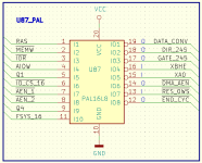
Where the PAL16L8 is not registered but it does possibly feature an /OE function. I see in the datasheet:
- 10 inputs
- 2 tri-state outputs
(0 registered Q outputs)
- 6 I/O pins

Pin 1-9 and 11 are inputs.
Pin 12 and 19 are the tri state outputs.
Pin 13-18 are the I/O pins.
This is important because the connections in the 5170 circuits to certain pins may provide important clues if those special functions are used.

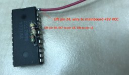
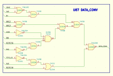
I attached a pin diagram of the connections to U87 here as example.
As we can see where I noted in the diagram at certain pins in the blue text, certain I/O pins were defined as inputs by IBM.
I am not sure if this needs to be specifically listed in WinCupl?
Maybe it does and that's a potential cause of my problem that the 5170 cannot function with the GAL? Though I didn't get any compile errors. I need to learn a few more additional details possibly if this is the case.

I see in the datasheet that there are certain points in the fuse map of the "PAL"L8 types which provide possible connections to each output to provide an /OE function for each pin, if it is optionally programmed to use a /OE function for the pin.
So theoretically any input or other point in the logic equations can provide an /OE function on any of the outputs.
So a certain input or logic statement could provide this. I must say, I have not observed any tri-state behaviour but I don't think that this can be actually observed in my test PCBs. My outputs use a simple 74LS04 inverter to provide LED indication. I should probe the voltage of the outputs without the 74LS04 plugged in so they are not influenced by the LS logic inputs of the 74LS04. Possibly this /OE aspect may complicate things for me now so I should check this on the 5 outputs.
I may have documented the behaviour of the PAL not knowing whether some result is caused by a tri-state situation or not.
I need to look at the connection in the 5170 to see if tri-state could be used anywhere on those outputs in the circuit. I think they are all straight inputs to be driven by single source outputs in those nets.

I will also probe the programmed GAL chip in full detail with the same diagrams I used for assembling the schematic I posted earlier to compare if the GAL behaves 100% identical after programming to what I have observed in the IBM chip so far.
 

Attachments

  • U87_PINS.png
    U87_PINS.png
    12.1 KB · Views: 4
  • PAL16L8 logic diagram.png
    PAL16L8 logic diagram.png
    146.9 KB · Views: 8
I forgot to post my WinCupl source file, here it is what I have so far, do note that this is not a functional solution -yet- here at this post if anyone arrives here by doing a web search.

Code:
Name     IBM-5170-U87 ;
PartNo   00 ;
Date     30-12-2023 ;
Revision 01 ;
Designer Rodney ;
Company  - ;
Assembly None ;
Location None ;
Device   G16V8A;


/* *************** INPUT PINS *********************/
PIN 1=RAS;
PIN 2=MEMW;
PIN 3=IOR;
PIN 4=AIOW;
PIN 5=Q1;
PIN 6=IO_CS_16;
PIN 7=AEN_1;
PIN 8=AEN_2;
PIN 9=Q4;
PIN 11=FSYS_16;
PIN 13=RES_0WS;
PIN 15=XA0;
PIN 16=XBHE;


/* *************** OUTPUT PINS *********************/
PIN 12=END_CYC;
PIN 14=DMA_AEN;
PIN 17=GATE_245;
PIN 18=DIR_245;
PIN 19=DATA_CONV;


!END_CYC = ((!IO_CS_16 & Q1) & !(IOR & AIOW)) # ((AIOW & !RES_0WS) # (!RES_0WS & RAS) # Q4);
DMA_AEN = AEN_1 & AEN_2;
GATE_245 = !(DMA_AEN & XA0) # ((DMA_AEN & XA0) & (MEMW & !RAS));
DIR_245 = !DMA_AEN # XBHE # (MEMW & !AIOW);
DATA_CONV = !(((!(XBHE # XA0)  & Q1) & (DMA_AEN & !(!AIOW & IOR & ((IO_CS_16 & !RAS) # (IO_CS_16 & FSYS_16))))) & ((!FSYS_16 & RAS) # IO_CS_16));
 
I have disconnected the PAL outputs completely in my test PCBs and measured pin 12 and 19 with a scope.

Next I applied various input combinations which I know change the states of these pins.
And several others just for measurements.
So far I have only seen the logic 0 and logic 1 states happen at any time on these two outputs.
Since the mention in the specs is that there are only those 2 outputs which could possibly go tri-state floating if this were programmed.
I didn't notice any undefined states, the two pins measured only had a connection with the scope, nothing else so it's only the PAL controlling those connections.

I possibly have some additional things which are yet unclear and I may need to learn but I found some old data books about PALs which seem to contain a lot of information, which of course is also at the same time the problem. If I find other relevant info which might be important in this case I will share it here.
 
I have been probing U87 a lot with my test PCB setup and I discovered several more product terms in most of the outputs of the PAL.

Here are my latest findings in WinCupl source code format:

Code:
Name     IBM-5170-U87 ;
PartNo   00 ;
Date     31-12-2023 ;
Revision 02 ;
Designer Rodney ;
Company  - ;
Assembly None ;
Location None ;
Device   G16V8A;


/* *************** INPUT PINS *********************/
PIN 1=RAS;
PIN 2=MEMW;
PIN 3=IOR;
PIN 4=AIOW;
PIN 5=Q1;
PIN 6=IO_CS_16;
PIN 7=AEN_1;
PIN 8=AEN_2;
PIN 9=Q4;
PIN 11=FSYS_16;
PIN 13=RES_0WS;
PIN 15=XA0;
PIN 16=XBHE;


/* *************** OUTPUT PINS *********************/
PIN 12=END_CYC;
PIN 14=DMA_AEN;
PIN 17=GATE_245;
PIN 18=DIR_245;
PIN 19=DATA_CONV;


!END_CYC = ((!IO_CS_16 & Q1) & !(IOR & AIOW)) # ((AIOW & !RES_0WS) # (!RES_0WS & RAS) # Q4);
DMA_AEN = AEN_1 & AEN_2;
GATE_245 = !(!(FSYS_16 # XBHE) & XA0 & DMA_AEN) # (!(FSYS_16 # XBHE) & XA0 & DMA_AEN & MEMW & !(IO_CS_16 # RAS));
DIR_245 = (!(!AEN_1 & RAS & MEMW) & !DMA_AEN) # (XBHE & DMA_AEN) # (!AIOW & DMA_AEN & MEMW);
DATA_CONV = !(((!(XBHE # XA0)  & Q1) & (DMA_AEN & !(!AIOW & IOR & ((IO_CS_16 & !RAS) # (IO_CS_16 & FSYS_16))))) & ((!FSYS_16 & RAS) # IO_CS_16));

Up to now no luck and the 5170 mainboard was not getting to a POSTable state yet so far.
I have not updated the schematic but I have the schematics in a logic simulator to compare them with the IBM PAL each time.
After I have the complete signals I will update the schematic in a final form.

Right now I am having another idea since these new product terms keep adding up and not all of them appear to be found.

Since I have a large portion of the product terms presently documented and implemented in my test GAL, the number of missing terms are subsequently decreasing.
I will make a test PCB where I will read both the IBM PAL and my test GAL side by side as one normal EPROM, taking the 4 complex outputs of both the PAL and the GAL as the first and second nibble of each "EPROM" byte.

Theoretically if reading them out goes well, I would then be able to compare each set of hex nibbles with eachother and spot all the differences.
After finding these I can convert them into product terms and try to complete the equations.
So that's my plan now, I will wire up a PCB today and try it out.

I saw a slight delay after applying power to the PAL and GAL before the LEDs would show an updated state so I will apply the VCC power with my own power supply and let the Galep-III read the logic states only.
I am not sure if the programmer can cooperate with my plan but I will update it here.

Another idea I have is to probe all the outputs of the IBM PAL in operation in the 5170 mainboard.
This could allow me to spot any tri-states of pin 12 and 19 inside the 5170.
This another plan after I do the EPROM method.

Since my situation of reading PAL data is very specific, I will not be wiring the EPROM setup using resistor networks, instead I will wire the 13 inputs and 4 complex outputs together as one 16kb EPROM.
 
I now have a tool to check whether my GAL is a match with the IBM U87 PAL, which is a step forward to getting there.

So this is the table of signals of the code read into my bin file as a ROM:

Code:
TEST GAL OUTPUTS:   IBM U87 PAL OUTPUTS:
=================   ====================
D4  /END_CYC_1      D0  /END_CYC   
D5  GATE_245_1      D1  GATE_245
D6  DIR_245_1       D2  DIR_245
D7  DATA_CONV_1     D3  DATA_CONV

INPUTS:
=======
A0  RAS   
A1  /MEMW   
A2  /IOR
A3  AIOW
A4  Q1
A5  /IO_CS_16
A6  /AEN_1
A7  /AEN_2
A8  Q4
A9  FSYS_16
A10 /RES_0WS
A11 XA0
A12 XBHE

Code:
                                   DDGE  DDGE
                                   C22C  C22E
                A AA               
                1 11AA AAAA AAAA   GAL   IBM U87
                2 1098 7654 3210   7654  3210
200     FD      0 0010 0000 0000   1111  1101 (FD)

Here in this example read out of the GALs FSYS_16(A9) going high and other input signals staying 0 should result in GATE_245 going active low which I will need to add to the GAL logic.
This condition comes with several dependant inputs which also need to be in certain logic states otherwise they will disable FSYS_16 to activate GATE_245.
These dependancies also need gates to decode them in the circuit so no unwanted conditions can happen.
Which is what I have been working on and doing logic simulations.

Because of including more and more product terms I am getting to a point where the limitations of how much code can fit inside a GAL is starting to come up.
When compiling the equations, WinCupl is reporting this with a compile message:

0006cc - excessive number of product terms: "variable"
"The number of product terms needed to implement the logic expression for the given variable exceeds the capacity of the output pin for which it was declared."

The limit of the combinations possible with a GAL are starting to become involved now.
However we already know that it must be possible to implement everything, so this is also a kind of assurance that there must be a way to do it.

So I have to look at the problem from all different angles to find where the simplifications can be found.
I will start doing this with GATE_245, which is the first signal that is now creating this compile message.
I have tested, even removing a single variable allows it to compile.
It all comes down to reducing the amount of gates needed so it becomes possible within the GAL fuse map ability.

If anyone has some ideas feel free to share them.
I will keep working on this problem, I hope I can achieve the full IBM PAL functions in my GAL.
 

Attachments

  • U87 IBM VERIFY 002.zip
    703 bytes · Views: 1
I can't get WinCupl to cooperate, it seems to take too many terms to compile the code.
I tried several approaches but still come up short on the internal gates in the GAL according to WinCupl.

I tried to create the source and compile a .jed file of the extracted equations found on this forum, just for a test and compare, however when I rewrite them to WinCupl code, the compiler throws a different error. I suspect it is trying to use one of the inputs as an output to assemble the connections and then throws an error "The variable used as an input was previously assigned to an output that is neither bidirectional nor feeds back into the input array.".

In short, WinCupl is not working out for my purpose. I will try PALASM in a dosbox environment, to see if this can provide me some solutions.

I am already thinking one step further, I had better look into using some CPLD type of 5V tolerant chip which is more modern and comes with better tools and compilers etc. At least this way I can assemble all the logic I want and be sure to achieve the functions that match U87 100%.
Without the original design specs by IBM it's much harder to assemble a working logic that matches the original PAL. After all, it may even contain some outputs which are not going to happen in reality, and were perhaps considered not a problem before. Looking at things backwards is always more complicated. Learning to use a CPLD will always come in handy for future projects if they become more and more complex and fast.
 
Current production 5V CPLD? Atmel/Microchip still produces the ATF1502 and ATF1508, supersets of the old Altera MAX7000 series EPM7032S and EPM7128S. JTAG in-system programmable with Atmel/Microchip's programmer. You can do the design in Altera's Quartus II, no later than version 13.0 sp1 and convert to ATF150x with the 'pof2jed' program, then program with ATMISP.

There have been some attempts at reverse engineering the fuse maps for these, as well as using the Atmel fitter in an open source tool chain built on yosys. May be overkill for this, but I could see an ATF1507AS replacing a lot of logic.
 
Hi lowen,

Thanks a lot for your advice, I will definately check up on your suggestions, hopefully I can find a good source for this type of CPLDs so I can use one in my project. Arguably I could possibly still use some PALs but I think it would also be much more beneficial to get into CPLD programming as well because I am seeing the component counts go up a lot.

Since I can't retrieve the original PAL code anyway, I should just focus on achieving the same function, and when things are completely matching in my output compare method which I described here, I can look more at gate reduction which may or may not produce a final simplified design. If that design would be simple enough to fit a GAL after all, I will do that for the sake of preservation. I will be able to say more about this later on.

For the people finding this thread using a web search I will add some important things to your suggestions in order for the next persons to save the time which I have spent for getting started.

So I have also done some research myself in the mean time before seeing your post lowen. After failing to find useful info on some google searches I remembered that these days you can find more useful info on youtube, or even TikTok? But I have not tried the latter yet because I like to follow up on content and see who posted and what channel etc.

The problem like with all retro tech is that the industry has since moved on and doesn't care about the stuff they left behind, which is of course their own history and legacy. To people like us this legacy matters.

So I searched on youtube. I saw Bil Herd do some videos for hackaday years ago where I saw on his screen in the video that he used the EPM7064SL44 which is the family type of "MAX7000S" in Quartus.

Next I already had a hard time of course finding anything useful on the website of Intel who took over the business from Atmel. The oldest version of Quartus I could find for download at their site is 13. So I tried that one, however I could not see the device selectable for MAX7000S for a project. Since I could see in the video by Bil that it was however possible to select this chip family in Quartus, so I searched for even older versions. The closest I could find that is older than 13 was version 11, so I installed that one.

In Quartus version 11 thankfully I could finally select the MAX7000S family and I was pleased to see 5V logic and a PLCC or QFP type package of 44 pins, which is more fitting for my project.

So Quartus version 11 can support many more older CPLDs, so people into retro tech can know this hopefully before doing many searches and installs of gigabytes of FPGA software to find out which takes hours of time.

The MAX7000S will be pretty fast I am sure, maybe 10 times faster than a GAL so I may be facing propagation problems, which however can possibly be measured by a dual channel scope to see the actual propagations happen. If these times can be measured this can then be compared with the IBM PAL in operation to get an idea. Anyway, I hope that such elaborate work may not be necessary, however I am thinking ahead a little.

I didn't have time yet to work in Quartus, however I see it has a nice schematic editor. Of course, at some time I will need to dive into the rabbit hole of VHDL and Verilog, but this will be an even longer track. I am already sensing that observing an output change while probing the PAL would be much easier to add in VHDL so frustration with the logic gate method may drive me into doing it in VHDL code instead. I do own a book about this however I wonder how long that will take and delay my project even more. I will see if using logic gates will be sufficient for now, I am trying to develop a method of description of behaviours which then translate into groups of logic tied to eachother. To have a method also saves time.

Anyway, I appreciate all past and future suggestions, thanks!
 
Last edited:
Yes lowen, so actually what you suggested and what I found is basically the same family of programmable logic, so this is what I need to learn to program and use.

I think what you were suggesting is to generate a design in Quartus 13 and create a design file, which you then convert with pof2jed software and use a USB blaster?

I hope I could do it in one single step if I could use Quartus 11 which I have found. I am not sure because I have to do a lot of preparation to get the complete design in, and then obtain some chips and a USB blaster. Next it will be troubleshooting and debugging. It's a lot more work than using the GAL which didn't work out. Since the GAL is already being reported to max out on certain equations I feel it's not a good idea to stick with it because the GAL version is still not complete so it needs more gates. What I am suspecting is that for example in the GATE_245 output there is some possible connection between different branches of gates which reduces the total amount of logic needed. However unless I find it that won't be an option.

So it's more difficult but in the end it will be the more sure path to use CPLDs. I will need to make some adapters for programming and for plugging the resulting CPLD into the 5170 connections for final testing.

I will see if I can implement both the PALs in a single CPLD after U87 is done, and probably more circuits such as DMA interfacing which needs to be as fast as possible in the decoding parts, which will make it worth my time and extra effort even more to use a CPLD. Faster timing in the DMA circuits will make the PC much more stable which I also experienced with my XT mainboard.

Anything I move into a CPLD will first need to be tested in my 5170 as much as possible so I can know if the timing is not too fast which is also possible. The more problems I exclude before hand the better which is what I also did in my XT designs.

I will proceed to enter all the gates of my latest versions of the U87 outputs into Quartus, and compare the results in a logic simulator first to make sure it matches my latest findings. I will see if I can obtain some CPLDs and a USB blaster in the short term which can save a lot of time in the whole process.
 
Last edited:
Glad to be of help. I'm actually currently looking at a MAX7128S design, and looking for current production parts myself; I have a small stock of EPM7128S in the 100-pin QFP package, but if the device I'm working on goes into production I'll be sourcing the Atmel ATF1508AS as a direct replacement.

Atmel and Altera are two different companies; Altera was acquired by Intel, Atmel was acquired by Microchip. The Atmel/Microchip parts are current production and can still be ordered new through Digikey and Mouser; see for instance the Digikey page for the 84 pin 15ns PLCC version of the ATF1508AS at https://www.digikey.com/en/products/detail/microchip-technology/ATF1508ASV-15JU84/1008617

The MAX7000S chips can be programmed by used Quartus II 13.0 sp1; there is a 13.1, but MAX7000S/EPM7xxxS is no longer supported in 13.1. They are supported in 13.0 sp 1. You can find a copy of the datasheet at https://edg.uchicago.edu/~bogdan/l1aux/doc/parts/m7000.pdf

MAX7000S series chips are no longer in production; you can still find them on eBay and other places, but the functionally equivalent (once programmed) ATF1502, ATF1504, and ATF1508 are still available in new production. ATF1502 is functionally equivalent to MAX700S-series EPM7032S; ATF1504 is functionally equivalent to EPM7064S, and ATF1508 is functionally equivalent to EPM7128S.

To program an ATF150x chip you CANNOT use the Altera programmer; you have to use the Atmel/Microchip programmer. For more information on the Atmel/Microchip ATF150x series prgramming, see https://ww1.microchip.com/downloads/en/DeviceDoc/doc1936.pdf and https://ww1.microchip.com/downloads/en/DeviceDoc/Atmel-8968-CPLD-ATF-ISP-User Guide.pdf - the short version is you need the ATMISP software and the ATDH1150USB USB programming cable with the appropriate header on you board or a programming jig.

I have an Altera USB blaster programmer I got with an Altera UP2 development board (EPM7128S and FLEX10K development; FLEX10K is last supported in like Quartus 9.x). I have successfully done a couple of test setups using Quartus 13.0 sp 1 (NOT Quartus 13.1), and it works fine. But when I go to the ATF1508AS I'll have to get the Atmel ATDH1150USB cable and use ATMISP, since the programming algorithm is different between the Atmel and Altera parts.

Quartus can't directly program the Atmel parts, but is a much better design environment than the Atmel-supported WinCUPL. You CAN get Atmel's ProChip designer, but it's commercial software and relatively pricey. But you CAN generate the POF files used to program the Altera MAX7000S parts and then convert, using POF2JED, into files ATMISP, the Atmel programmer, can then program the Atmel parts.

There's a lot of information out there about using the ATF150x parts in a MAX7000S toolchain; what I've written really just barely scratches the surface.
 
Back
Top