• Please review our updated Terms and Rules here

8-Bit IDE Controller

Here's a utility that will help with this debug.
It has already shown me an error on my system too.

http://www.waste.org/~winkles/int13test.zip

This dumps out the drive parameter table(s) as well as what int 13 fn 48 and 8 report back.
What I need folks to do is take a drive, preferably 10G or less and put it in a modern machine. Run this program and redirect the results to a file.
Do the same on your XT. If the results are different, send them to me.

I've already seen a bug on my end with this tool, and that could very easily be what is causing your problems too. hopefully I can dig in shortly.

---------------------------

Good news!
I've finished card #5 and it worked right out of the shoot.
I also gave a workover to cards #1 and it is now working as expected.
Card #4, the one that was dropping case on the ID string worked at least 1 time tonight (I swear!), but is now back to dropping the characters again. It's really weird indeed.
So I have two cards at the moment that appear to be as good as all the others, and one that works, but works a little wonky.
---------------------------

Bad News!
I have 2 more bad eeproms. Either these SEEQ parts are just really horrible, or I've managed to wreck 3 parts now, possibly due to card #1 being troublesome.
That makes 3 bad eeproms out of 11 that I purchased for this project. (1 went to bob watts)

So, if we get any programming failures in the immediate future from BIOS upgrades, I suggest we dump these SEEQ parts and find something else, like the atmel's that were working just fine from the wire wrap cards.

that's it for me tonight.
 
Last edited:
Hi! I agree. With the latest test results I think we are probably past the big hump on the PCB prototype. We need some testers who are going to beat on this design and drive out the bugs. I mean some ruthless beat down testing. If there are people willing to test lets have a go at it and get as much value out of these initial test units as possible.

Thanks and have a nice day!

Andrew Lynch

Ok, I think I might squeak by as a qualified tester and, since I've set up an XT testbed to run all the 8-bit cards I have to still test through, I can give it a real world shakedown with a LOT of strange cards to see if it fouls up somewhere and put a good number of miles on it.
 
Hi Per! I was thinking that to get the interleaved HIGH/LOW reading from a single IO port that was to use a 74LS74 flip flop on the latches chip select line for the latches. A reset signal would clear the flip flop, then the first read would give HIGH, the next LOW, the next HIGH again, and so forth. Eliminate the use of the A3 line and just use the flip flop output to toggle back and forth. (74LS74 configured as JK FF with direct clear)

What complicates matters is that the IDE chip select signals cannot be asserted during the DMA transactions. So they would have to be qualified (with 74LS32 and probably a 74LS04 inverter) with the DMA status lines. This gets complicated since there are two separate IDE chip selects.

Here is some information from the IDE "standard":


http://www.ele.uri.edu/courses/ele408/s2001/projects/roland_ide/IDE.pdf

I am fuzzy on the whole DMA implementation to begin with so whatever design does finally surface would require some test with a prototype board to ensure it really works. I see this easily adding several chips to the design which is why I believe the GIDE developers ended up using GALs to keep part count reasonable. If adding DMA capability comes at the price of doubling part count I do not think its worth it as it would dramatically increase unit cost due to additional parts, larger PCB required, etc. There are benefits to keeping this simple and cheap!

Thanks and have a nice day!

Andrew Lynch

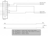
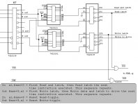
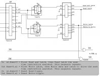
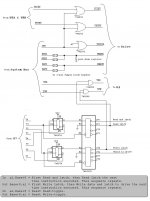
I've made some schematics. I've using the more flexible 74LS161 counter, but if a flip-flop will do, it'll problably be better. Currently, it just adds 4 IC's to the design.

About the not-assert-thing, we can invert the AEN signal and AND it with the lines we need to hold low when DMA is being active. If it need to be held high, an "OR" with a non-inverted AEN signal is enough.

Anyway, take a look at the schematics for my solution about how to read it all from one port (one is how it is now, the other one is my idea).
 

Attachments

  • DMABefore.JPG
    DMABefore.JPG
    38.5 KB · Views: 1
  • DMAAfter.JPG
    DMAAfter.JPG
    70.8 KB · Views: 1
Last edited:
please, Please, PLEASE make a posts-in-progress-to-be-temporarely-saved-on-posting-failure function! This is the third time I write this post :mad:

sorry for yelling...

---

I suggest you put a pull-up resistor on the line after J2. Else, we can't guarantee that the /WE goes high.

Writing a program to search for free memory in the upper areas is easy, but doing the same for I/O addresses might cause troubble. If you read from a write-only port, weird stuff may happen. You also have ports that returns 00h by purpose. I would suggest setting the card to the settings reserved for the fixed disk controller (according to the tech-ref: I/O port 320h, Base addres for ROM at C800:0000, and IRQ 5) and just assume the user reads the manual.

Adding DMA-compability problably adds something between $5 and $10 to the total costs. I've already replaced the counters with flip-flops (with /Q tied to D, see the updated schematics) so that reduces the chip-count by one. This means that the additional chip-count is 3 plus what-we-need-to-ajust-CS (one or two extra ICs), hence the total additional chip-count won't be more than 5 ICs.

In addition, we need somebody that's able to add DMA capabilities to the BIOS as of neither me or Hargle really knows how to program with DMA.
 

Attachments

  • DMAAfter.JPG
    DMAAfter.JPG
    66.5 KB · Views: 1
Writing a program to search for free memory in the upper areas is easy, but doing the same for I/O addresses might cause troubble. If you read from a write-only port, weird stuff may happen. You also have ports that returns 00h by purpose.
Unused ports return FF, just like unused memory, so if you see 00, you should skip it. There shouldn't be too much in the 200-300 range to cause us problems (just add on cards), and the idea is that you run this program and then power off to insert our card, so even if we put the machine in a bad state, we're power cycling anyway.
Unless it completely locks up the machine to read from a write only port, the program should be able to do what it needs to do. Either way, this is only a helpful program for inexperienced users to mess with.

In addition, we need somebody that's able to add DMA capabilities to the BIOS as of neither me or Hargle really knows how to program with DMA.

The only DMA work I've done is on a soundblaster 1.0 card.
http://www.waste.org/~winkles/hardware/soundblaster/sb.asm

I do twiddle the DMA controllers directly to do the transfer, but how it actually operates in the hardware is beyond me.
I should see if that code works on an XT. I've only ever tried it on a 386 or better, but it is using 8086 friendly code.

I plan on using some of the routines from that code for the IRQ detection, and if we play with DMA, that code should also come in handy.

--------
I've got this book called "the undocumented PC" and it describes in pretty good detail how a DMA transfer is done from an adapter card into memory.
Should I type it up?
 
Last edited:
What needs to be done in the BIOS to add DMA support?

I really don't know, but I think we have to make the drive aware that we're doing DMA transfers.

I don't know really well how DMA works (neither software or hardware), but I know it has something to do with doing multipile IO port reads from one port with a piece of memory as the destination.

If I only knew how the chip select signals are used... Should they be held high or low when DMA is active?
 
I really don't know, but I think we have to make the drive aware that we're doing DMA transfers.
I was thinking you were referring to the mainboard BIOS, hence my confusion and my edit later. (my bad)
I should reiterate that I've done DMA transfers on other hardware. If you guys get the hardware to work, I will absolutely get it working in the bios! :)

Here's the writeup from undoc PC:

A typical I/O to memory transfer:
This shows the sequence of events when a DMA is initiated, performing a data transfer from an adapter card's IO directly into memory. This is considered a DMA write. DMA channel 3 is used in this example, (hargle: which is good, cuz that's the DMA channel for HDD!) and no other DMA transfers are in progress.

The complete processing of this transfer occurs in the following sequence:

1) a device driver (BIOS) initialization routine programs the DMA chip, setting up the following information:
Base address in memory where the 1st write should begin. The lower 16-bits are programmed in the DMA controller, channel 3. The upper address bits are programmed into the page register 3.
Count of bytes to transfer on the request, less 1, is placed into the DMA controller channel 3.
The transfer mode is selected as "demand mode"
The direction count is set to increment.
The transfer type is set to "write"
the DMA mask is updated to allow DMA Request 3 (DREQ 3)

2) The adapter card requests DMA service by asserting a high on the DMA request line (DREQ 3)

3) The DMA controller verifies that DREQ 3 is allowed, and then asks the CPU to go into a hold mode by asserting the hold request line (HRQ)

4) The CPU responds by asserting the Hold Acknowledge (HLDA) and goes into a bus hold state.

5) An address generated by the DMA system is passed onto the bus. The memory write and IO read control lines are also activated. The DMA acknowledge (DACK 3) signal is activated, so the adapter card is aware the transfer is now in progress.

6) The data is transferred directly from the adapter card to memory without passing through the DMA controller. The cpu interweaves normal cycles and bus holds cycles as the transfer proceeds, under control of the DMA controller.

7) The transfer completes when the DMA controller's count completes, or if the transfers are going too fast for the adapter, the adapter can temporarily hold the transfer by dropping the DREQ 3 line.

8) At completion, the DMA controller asserts the Terminal Count (TC) line to signal the adapter card that the transfer is complete. The Hold Request (HRQ) and the DMA acknowledge line (DACK 3) are deactivated.

9) the adapter turns off the request (DREQ 3)

10) The cpu resumes normal operation

--------------------------

#1 is all BIOS. No sweat on any of that.
#2 probably comes from the drive itself, asserting dreq when data is ready
#3 no concern for us
#4 no concern for us
#5 ?
#6 I'm assuming that if you can get 512 IO reads from a single port to transfer 1 sector of data, we're set here.
#7 driven from the drive, signals that the data is finished
#8-10 no concern for us.

So I think a big huge step toward DMA is getting all the data to appear via a single IO read. That would help speed up PIO as well, so that would be useful even if we go no further.
 
Hi! Based on the discussions I am starting to think we should just "snap a baseline" for the existing XT-IDE design with PIO+IRQ+BIOS. Then start a new development for a "Version II" model that supports DMA. I think we could spend a lot of time exploring DMA and not getting anything out. What we have is pretty good and is a >90% solution for most people.

Concentrate on getting the production XT-IDE board out "as is" and then focus on another iteration that supports DMA or other advanced features *if there is a need for it*. I know some people would like DMA and so would I which is why I looked into it but there appears to be so many unknowns associated with it that I believe it would interfere with releasing the good stuff we've already gotten. Besides, I think any design with DMA would need another round of wire wrap prototypes, new BIOS versions, etc.

Thanks and have a nice day!

Andrew Lynch

What is the transfer boost gained by DMA?

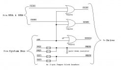
I have researched the document you linked to, and we actually only need to add one additional 74LS32 chip.

So in order to support DMA, 1 resistor, 4x 2-header jumper blocks, 4 capacitors, and 4 ICs have to be added (one 74LS74, one 74LS139, one 74LS08 and one 74LS32). This will also fix some issues that might appear since /IOCS16 is not connected to anything (since there is no problems yet, most drives problably got a pull-down resistor on this line).

Anyways, we could make a poll, where we ask if people would like to wait to see if the DMA version get successfull. About the wire-wrap prototype, you already got most of it already done since only some lines are redirected/altered/added. See below for the last changes that has to be made according to the document.
 

Attachments

  • DMAAfterMisc.JPG
    DMAAfterMisc.JPG
    28.3 KB · Views: 1
I might have posted stuff in a little too fragnemted way. Anyways, if DMA should be considered in the future, here is my solution to how to make the card compatible. It should theoretically work, so if there is any interest, I would recomend to try it.

Nothing of the existing schematics have to be removed, it's just additions.
 

Attachments

  • DMAFinal.JPG
    DMAFinal.JPG
    90.8 KB · Views: 1
I wish I could help you guys out with this card, unfortunetly, this stuff is way beyond me, if you need a beta tester I have give it a whirl though.


:D
 
Hi Per! I don't know the speed gains from DMA. They could be significant or they might be very little. DMA is a big deal on faster CPUs but on the older PC/XT systems it was less of an issue.

I like the idea of DMA it is just how to do it. I am sure that I don't want to further delay the project by chasing ever greater features while not ever getting anything out to the people who want it.

At a minimum, we need to resolve the unknowns about DMA and do some prototyping before making any decisions on DMA capability. We'll need working hardware and Hargle has to be able to use it to write a BIOS.

Probably a good approach would be to continue on the path we are on to a summer release of the current design and I modify Hargle's semi-working wire wrap prototype with the new DMA features. Once that's in place, Hargle could send me some test code to see if it works and if it does I'll send the prototype back to him for more BIOS tweaks.

I suggest this be done in parallel with the current design as there may be some surprises resulting in delays, etc.

Thanks and have a nice day!

Andrew Lynch
 
I suggest this be done in parallel with the current design as there may be some surprises resulting in delays, etc.

Thanks and have a nice day!

Andrew Lynch

That's a good idea.

Just make sure to keep us notified if you get my schematics to work ;) .

---

About DMA speeds, one transfer takes 5 clock cycles. Each clock cycle takes 210nS, so each byte-transfer takes 1.05uS

So teoretically, with DMA, you can transfer 1 000 000 / 1.05 bytes per second. That's just a little less than 1Mb/s.

However, the DMA controller of the XT can't transfer more than 64 Kb at a time, so this will have an effect on the transfer rate. There are other stuff affecting the rate too (like DRAM refresh), but rates up to 300kb/s should be possible after my guess.
 
Probably a good approach would be to continue on the path we are on to a summer release of the current design

Ahh, the voice of reason :D

I agree with Andrew that DMA is something that can be implemented in version 2 of the card.

With that being said, how hard would it be to incorporate a Floppy controller into this design so that they were on one card? Not saying you should, I am just curious about its feasibility.
 
please, Please, PLEASE make a posts-in-progress-to-be-temporarely-saved-on-posting-failure function! This is the third time I write this post :mad:

sorry for yelling...

---

I suggest you put a pull-up resistor on the line after J2. Else, we can't guarantee that the /WE goes high.

[snip]


Hi Per! Thanks! Great catch!

Thanks and have a nice day!

Andrew Lynch
 
I concur with the thought of cutting the development of DMA for now and getting this new board made up. Less risk, and will certainly work good enough for most people. Since the 1st round of 10 PCBs and parts weighed in at about $40 per card to build, I think if we pursued DMA and then did a tiny run of 25 cards or so, we could still get some buyers. Probably not 100 like we have for this design, or there's crazier people out there than I thought! :)

That said, do you think we can do a big run with the existing design, or should we do another run of 10 cards (or less), to make sure we're good to go?

I do want to see if pulling csel low causes any changes to functionality. if it doesn't, I'd like to get rid of that option altogether. that'll simplify the design and build process even more. I think we may want to wait til the last minute to pull that feature out, just so we don't confuse functional changes with any BIOS bugs that we're now discovering...
 
I'm sure it's a dumb question but is the intent that we (users of the cards) use an additional/external power supply for the hard drive? (ie for systems that can't handle that load)
 
I'm sure it's a dumb question but is the intent that we (users of the cards) use an additional/external power supply for the hard drive? (ie for systems that can't handle that load)

If you replace a fixed-disk with this card and an IDE drive, the load will acutally be a lot less than with the original MFM drive.

Reasons for this is mainly because of a smaller chip-count on the interface card, and that the IDE drives are smaller than the noisy full-height drives.
 
Back
Top