• Please review our updated Terms and Rules here

Cromemco dazzler replica project

I was looking at the memory board S-100 bus signals to see if there was an obscure one that was not being generated by the Dazzler.

I did find one, only to find that this signal is weirdly generated by only one bus master (the ZPU). This signal, in turn, is derived from two S-100 bus signals that are produced from the Dazzler.

I think we can also rule out DRAM cards as a swap.

Dave
I never got to try the dazzler with DRAM, but I figured that the refresh activities on a DRAM card would corrupt the function, at least give snow at worst not work.
 
I think I have found the issue. It is with the memory board (well, the Dazzler DMA cycle is not compatible with the operation of the memory board).

Hugo, can you check my logic please?

It would seem that the memory board is equipped with SN74LS375 quad latches on address bus A0 to A15.

The clock (on pins 4 and 12) of these ICs is required to go HIGH to latch what is on the S-100 address bus into the latches so that the memory on the card can be addressed.

This pin is sourced from the logic embedded inside 6C (so I can't see what it is).

The Dazzler DMA cycle sets up by 'forcing' the S-100 control signals to a fixed value and then just cycles through the requisite addresses by changing just the S-100 address bus and not the S-100 control bus.

I don't see a clock being fed to IC 6C, so I suspect that the address latches will latch in whatever rubbish happens to be on the S-100 address bus when the DMA cycle starts. This will invariably be FFFF...

Gut feeling is this memory board is not compatible with the Dazzler...

Having just written this post, I have reread the data sheet and it looks like the 'latch' pin is a logic HIGH level. So if this pin is held HIGH, the SN74LS375 should go 'transparent' - so this 'should' work now...

A second opinion required...

The strobe line is active LOW. As a result, the latches will be transparent UNTIL the /DATA STB signal goes LOW. At this time, whatever is on the S-100 address bus will be latched.

In order for the latched address to be updated, the /DATA STB signal must go HIGH then LOW for the next address. If the S-100 control signals never change state, and there is no clock involved, this will not happen.

The S-100 address bus may not be driven by the Dazzler at the time it takes over the S-100 bus and drives the control lines to a permanent memory read cycle.

A third opinion required now!

Dave
 
Last edited:
Here is a random thought...

Let's use the ROM code in the 16FDC (at a base address of C000) to act as our 'random' display data...

Use RDOS to enter the following commands (no need for my test program thus time)

O 0E E0
O 0F 19

This should enable the Dazzler, set the display memory base address to C000 (port 0Eh).

Set normal resolution mode, 512 bytes of display memory in colour (port 0Fh).

Incidentally, I checked the schematics for the Cromemco 4KZ static memory board. This still uses address latches, but includes PHI2 in the logic train - so this will guarantee a cyclic latch signal to the address latches.

There is an interesting write up here regarding the Dazzler compatibility with 'none Cromemco' boards: www.s100computers.com/Hardware Folder/Cromemco/Dazzler/Dazzler.htm. The URL has become split, so clicking on it doesn't work. Copy the text for the URL and paste it into your browser.

I suspect (from my investigation above) that the incompatibility is not the CPU board but the RAM board - and this is associated with the DMA cycles and RAM address latches. But that is just suspicion until validated. Intetestingly, they also mention the white screen...

Dave
 
Last edited:
Hey good morning! wow lots of info to absorb here, but did you still want me to try the tests in #758?
 
Oh well, worth a try...

But (interestingly) the screen is black and not white though...

Let me check my output commands...

Dave
 
I think I have found the issue. It is with the memory board (well, the Dazzler DMA cycle is not compatible with the operation of the memory board).

Hugo, can you check my logic please?

It would seem that the memory board is equipped with SN74LS375 quad latches on address bus A0 to A15.

The clock (on pins 4 and 12) of these ICs is required to go HIGH to latch what is on the S-100 address bus into the latches so that the memory on the card can be addressed.

This pin is sourced from the logic embedded inside 6C (so I can't see what it is).

The Dazzler DMA cycle sets up by 'forcing' the S-100 control signals to a fixed value and then just cycles through the requisite addresses by changing just the S-100 address bus and not the S-100 control bus.

I don't see a clock being fed to IC 6C, so I suspect that the address latches will latch in whatever rubbish happens to be on the S-100 address bus when the DMA cycle starts. This will invariably be FFFF...

Gut feeling is this memory board is not compatible with the Dazzler...

Having just written this post, I have reread the data sheet and it looks like the 'latch' pin is a logic HIGH level. So if this pin is held HIGH, the SN74LS375 should go 'transparent' - so this 'should' work now...

A second opinion required...

The strobe line is active LOW. As a result, the latches will be transparent UNTIL the /DATA STB signal goes LOW. At this time, whatever is on the S-100 address bus will be latched.

In order for the latched address to be updated, the /DATA STB signal must go HIGH then LOW for the next address. If the S-100 control signals never change state, and there is no clock involved, this will not happen.

The S-100 address bus may not be driven by the Dazzler at the time it takes over the S-100 bus and drives the control lines to a permanent memory read cycle.

A third opinion required now!

Dave
As you pointed out for the Memory Merchant 65K16S board, the S100 address signals A0-A15 are latched by 74LS375s. The 74LS375 is a "transparent latch" as long as its control inputs are held high. However, if the control input goes from a high-to-low transition and then stays low, the output becomes latched to the state of the input at the time of the transition.
On the 65K16S board, the address latch signal DATA_STB* is generated by an 82S100 FPLA. We really don't know what logic it uses to generate the DATA_STB* signal (perhaps a combination of sMEMR and pDBIN on cycles that have been qualified as memory reads) but almost certainly the DATA_STB* signal is not being held high all the time.

DMA as implemented on the Dazzler is very primitive. As you pointed out, the Dazzler does not attempt to replicate a normal S100 memory read bus cycle. At the start of a DMA cycle Dazzler simply forces the S100 status and strobe signals to a state required to read from memory, and then keeps those signals stuck there while it cycles through a range of addresses. This requires a memory board designed so that under those conditions its data output buffers are always on, and the data the RAM board puts on the S100 bus always immediately reflects the address that is on the S100 bus. The Dazzler requires a very basic RAM board - the 65K16S board is way too complicated for an application like this.

Most S100 dynamic RAM boards (perhaps with the exception of some made by Cromemco themselves) will not work with the Dazzler. They were designed to run a DRAM refresh cycle by "stealing" a bit of unused time at the end of every S100 bus cycle. The Dazzler reads a block of addresses in one pass with no attempt to simulate normal S100 bus read cycles, and leaves no unused time between each read of a memory address. S100 DRAM boards cannot handle this situation - either (a) poorly designed boards fail to refresh at all for the duration of time the Dazzler is reading RAM resulting in memory loss or (b) better designed boards with an internal "fail safe" timer force a refresh cycle to occur thus blocking access by the Dazzler.
 
Thanks for the confirmation.

I have just found out that the 16FDC ROM may not be a good bet for the Dazzler either!

There are wait states inserted if the ZPU is running at 4 MHz. However, the definition of "running at 4 MHz" is pin 98 of the S-100 bus produced by the ZPU. Unfortunately, this status signal is disabled during a Dazzler DMA access and this causes the bus signal to be set, thus making the 16FDC think that wait states are required...

Need to think again...

Dave
 
Are you able to scope the memory board easily?

If so, can you set-up our standard Dazzler test configuration again and probe the following pins on the memory card:

IC 12D pin 1.
IC 3A pins 18 and 20.
IC 6C pin 16.
IC 6C pin 10.

Dave
 
Are you able to scope the memory board easily?

If so, can you set-up our standard Dazzler test configuration again and probe the following pins on the memory card:

IC 12D pin 1.
IC 3A pins 18 and 20.
IC 6C pin 16.
IC 6C pin 10.

Dave

Yes I could do that, will be able to after some work calls.. :)

Also, FYI I do have a working 4FDC if you think that'd bring any more luck.. I have the ZPU running at 2 MHz.

Do you think any of those RAM boards I posted in #754 would stand a chance?
 
Last edited:
No problem.

Let's ignore the 4FDC for now. It would be another variable...

Let's see if we can work out why your memory card doesn't work (for fact) and see if we can modify it to actually work.

 Dave
 
Yes I could do that, will be able to after some work calls.. :)

Also, FYI I do have a working 4FDC if you think that'd bring any more luck.. I have the ZPU running at 2 MHz.

Do you think any of those RAM boards I posted in #754 would stand a chance?
The only board in your list that stands a chance of working with the Dazzler is the Vector Graphic 8K RAM - but I'd have to see the schematic to be sure, and I cannot find one for this board.

None of the dynamic RAM boards you listed will work. The "mystery board" you pictured is also a dynamic RAM board.

This should serve as a word of caution for anyone else who wants to build a Dazzler. The requirements for the RAM board it is used with are very specific, and even many static RAM boards will fail. The best CPU board to use with it is Cromemco's ZPU, and many other CPU boards will also fail to work properly with the Dazzler.
 
Last edited:
We know it works on a SOL-20 as well.

@Hugo Holden what is the configuration of your system out of interest?

Dave
In Holden's discussion of the Dazzler, he mentioned having successfully tested it with the "Seattle Computer" 16K RAM board, and the CompuPro RAM17 board (which is what I use).

Incidentally Mike Douglas had a batch of RAM17 boards he was selling a month ago and may still have some available if anyone is interested:
There is a comment at the end of the discussion linked to above, indicating the feature list of the RAM17 to be similar to that of the Memory Merchant 65K16S. While the feature list may be similar, these two boards are designed very differently.
 
Last edited:
Are you able to scope the memory board easily?

If so, can you set-up our standard Dazzler test configuration again and probe the following pins on the memory card:

IC 12D pin 1.
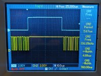
zoomed out slightly to 10us, to see the fully cycle. This pin goes high at our typical mark point, and goes low afterwards. At 5us timebase, its just slightly too wide to see the full thing.
PXL_20240401_165223126.MP.jpg
IC 3A pins 18 and 20.
18: no activity, stays HIGH
20: there is activity on this pin, goes LOW during our cycle

IC 6C pin 16.
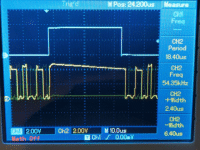
Ok, this looks....different:
ezgif-5-fb6bc30ca0.gif

IC 6C pin 10.
same pin 16
 
The only board in your list that stands a chance of working with the Dazzler is the Vector Graphic 8K RAM - but I'd have to see the schematic to be sure, and I cannot find one for this board.

None of the dynamic RAM boards you listed will work. The "mystery board" you pictured is also a dynamic RAM board.

This should serve as a word of caution for anyone else who wants to build a Dazzler. The requirements for the RAM board it is used with are very specific, and even many static RAM boards will fail. The best CPU board to use with it is Cromemco's ZPU, and many other CPU boards will also fail to work properly with the Dazzler.

When I drew out the PCB I didn't progress populating one as the N* uses dynamic ram and as such is supposed not to work with the Dazzler.

However the N* manual contains a note about modifications to work with the Dazzler with a DRAM board.

Modifications

SPECIAL DMA APPLICATIONS
This section describes modifications for the RAM-16-A which may be necessary for use with such DMA devices as the Cromemco DAZZLERTM. These modifications are only needed if the RAM-16-A is being used with a Z80 or Z80A processor board. (To use the RAM-16-A with a special DMA device in an 8080-based system, it is necessary only to install a resistor as described in step D1 below.)
 
Last edited:
Ignore the comment at the end of the discussion linked to above, indicating the feature list of the RAM17 to be similar to that of the Memory Merchant 65K16S. While the feature list may be similar, these two boards are designed very differently.

HAHA That comment at the end was me. Ignore, indeed. 😊
 
Those signals are not quite what I was expecting, but it does indicate why the RAM board is not working.

The data output buffer is not being enabled, hence the data bus (and therefore the Dazzler) is reading FFh (hence the white screen).

Neither is the RAM chip being enabled that I was expecting to be.

Think time...

Would you be up for pulling the two ICs I suggested on the Dazzler and doing a bit of temporary wiring?

 Dave
 
OK,

Select some wire that is thick enough to make good contact with the IC sockets, but not too thick to damage the sockets themselves.

Dave
 
Back
Top