• Please review our updated Terms and Rules here

2001-8 Chicklet Pet Fault Finding.

This additional trouble will make memories of fixing the PET even sweeter when you get it running.

How long was it working before the freeze? Minutes or an hour (thermal question)?

-Dave

Hi Dave the computer was only on for five minutes, just long enough to put the logic probe on and test the input pulsing and the out put pulsing.
It pretty much froze in the same way half the RAM died last switch on. The symptoms exactly the same where it just froze this time but last
time it worked then the cursor vanished and upon turn on lost half it's RAM 3071 to 1023.

It must be to much for the old girl, classic case of dementia in old age! Joking aside I'll take a look at the tynemouth solution.

Just out of curiosity why does the 6550 have a clock and four chip selects.

Oh is there any way to test the 6550's to see which are good for the video RAM?
 
Having a look at the schematics for the 2114 type memory with 6540 roms on the video ram,
the only difference seems to be the no clock signal and no need to tie the chip selects to 5v and only tying CS to gnd.
Does that mean you could replace video ram with 2114's all be it with adapters?

Regarding using 2114's for system memory is the only difference the addition of a 74ls139 doing the chip selecting?
 
Last edited:
It must be to much for the old girl, classic case of dementia in old age! Joking aside I'll take a look at the tynemouth solution.

Just out of curiosity why does the 6550 have a clock and four chip selects.

Oh is there any way to test the 6550's to see which are good for the video RAM?
Hi PR,
Having the 320008 assy board is good and bad news. Having original MOS Technology memory parts (65XX) make your PET the most desirable to collectors, but replacing them is a nightmare as they are made of unobtainium. Using socket adapters for all the memory will look kludgy anyway, so you might as well use a small RAM/ROM replacement board. You can keep the 6540/50 chips in place to make the PET look as original as possible.

The 6550 RAM contains only 1K of memory. So having several chip selects makes it easier map the chip into memory space without needing a lot of decoder chips. As for the clock, Static RAM chips should not need a clock, so I'm not sure. Perhaps the access time (time from address settling to data valid on output) of the device was so slow that there was a need to latch the address to hold it longer internally to the 6540.

If your two video RAM chips are on sockets, use trial and error when your PET is working and mark the good ones.
 
Does that mean you could replace video ram with 2114's all be it with adapters?

Regarding using 2114's for system memory is the only difference the addition of a 74ls139 doing the chip selecting?

Yes and yes. But replacing 16 main RAM chips with 16 adapters will look a bit kludgy. Some have used a single 8KX8 RAM chip. But realize there will be a nest of wires.
 
Yes and yes. But replacing 16 main RAM chips with 16 adapters will look a bit kludgy. Some have used a single 8KX8 RAM chip. But realize there will be a nest of wires.

Thanks for the info Dave and yours and KC's help with the cursor fault, your knowledge is invaluable to us rookies.
I am still learning as I go along and was interested in how the RAM was set up between the versions and
was looking at what you have just suggested with the 8k chip except I had been thinking of four 2k chips
so thanks for that info.

Am I right in thinking that each original chip has 4 bits of the 8bits in each bank. So if I was using less chips
I would just have four bits on I row and four bits on J on each chip and if using an 8k it would also be split
between I and J banks.(a0-a9 and d0-d7 across the two)

I like to use the repairs to gain a better understanding of electronics and these old beasts.
 
Am I right in thinking that each original chip has 4 bits of the 8bits in each bank. So if I was using less chips
I would just have four bits on I row and four bits on J on each chip and if using an 8k it would also be split
between I and J banks.(a0-a9 and d0-d7 across the two)

I'm not quite following your thought. The old static RAM chips were organized as 1K by 4 bits so two chips were necessary to get a full 8 bit byte. But now one can get up to 8K, 32K or 64K X 8 bits in one big chip. So only one chip is necessary. But the jumper wiring to the main board will be messy in order to hook up all the address and data lines to the right places. A RAM/ROM replacement board from Tynemouth or bitfixer is much cleaner.
 
the computer was only on for five minutes, just long enough to put the logic probe on and test the input pulsing and the out put pulsing.

I hope this was not somehow the infamous "Operator Induced Fault" that plagues us amateur technicians (as for me, I can design 'em, but better keep me away from testing 'em). Just in case, from now on take extra care on attaching the power and ground leads to the logic probe so that the clips cannot touch other signals or the chassis. Also it is quite easy for the probe tip to slip and short together two adjacent pins.
 
I hope this was not somehow the infamous "Operator Induced Fault" that plagues us amateur technicians (as for me, I can design 'em, but better keep me away from testing 'em). Just in case, from now on take extra care on attaching the power and ground leads to the logic probe so that the clips cannot touch other signals or the chassis. Also it is quite easy for the probe tip to slip and short together two adjacent pins.

No induced error luckily, the logic probe I use has a guard to stop you shorting two pins out and I put the supply pins on two separate regulators. (I shorted out a couple of pins once on a 6809 on an arcade board that burned out a trace, it taught me big a lesson) The night I bought it I swapped the 6550's around to get it working. Turned it off, turned it on and the next day the pet had boot screen with some extra garbage characters so I think it just doesn't like working!:D

Regarding the chips what I mean is that as the 1k 8bit word is split across I an J rows so for 1k you needed two 1k 4 bit chips per 1k of memory hence 16 chips. So would it be right to say if you use a 1k 8bit chip you would need to split the lines across the two rows I and J and only need 8 chips.

So using a 8k 8bit chip you would need just one split it across the two rows I and J that is if you plug into existing RAM sockets, I hope I am making sense:confused:
 
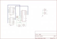
Dave on the subject of 6550 ram adapters I stumbled across this on the net but I am puzzled why it uses a 74ls00 to combine the clock with r/w signal?

http://vic-20.de/x1541/hardware/adaptors.html

I didn't think you would need the clock as the RAM chip doesn't need it or am I missing something?

I don't see the schematic, but the NAND gates may be used to form a WRITE pulse or even an Output Enable for the tristate control of the data lines during READs.
 
I don't see the schematic, but the NAND gates may be used to form a WRITE pulse or even an Output Enable for the tristate control of the data lines during READs.

Here's the schematic Dave:-

6550.jpg

I was wondering because the difference in schematics for 2114 and 6550 video rams, the only difference in the circuit was no clock signal to the 2114.
So I was wondering why the designer combined the signal when commodore disregarded the clock line for the 2114 version.

To ask another question when chips have more than the 10 address lines do you just tie the ones over A9 to 5v?
Just noticed on the schematic the combined signal is going to address A11 as well as WE and A10 is grounded?
 
Last edited:
You can tie the unused address lines up or down, it doesn't matter. Just don't leave them float.
 
You can tie the unused address lines up or down, it doesn't matter. Just don't leave them float.

Cheers for the info KC! How did you learn about all these topics? I did electronics many moons ago but it was mainly op amps diodes etc.
We did very little logic circuitry, only touched on it a bit with karnaugh maps etc to make a simple alarm and reduce the number of logic gates!
We did emma board 6502 programming and architecture but very little on utilising the address bus, ROM's and Ram timings etc.

Am I right in thinking the address lines tell the RAM where to put it's data via Rows and Columns.
 
Mostly reading and playing with these things since the early 1980s. I checked out every single technical book on computers that our local library throughout the whole 198x decade. The only thing missing was a librarian named Shardovan to admit that the technical section wasn't very large so I wouldn't waste all that time searching.

I've forgotten far more than I can recall. In fact, I've forgotten the internal workings of RAM. But I can tell you that if you have too many address lines, you have more RAM than you can use. Tying the extra lines down or up just causes you to use one section of the RAM. If you leave them float, you could be switching which areas you are using at random.

What would be slick is controlling those extra lines with a PIA or VIA. You could use all that extra RAM, by swapping banks.
 
I need to do a fair bit of reading, I have been messing with electronics for years but never had more than the basics back at college.
It is as you saying playing around with these machines and looking at schematics when you learn fast and start to understand more.
I look forward to buying a machine and find it's faulty so that I can learn how to fix it!
 
View attachment 32984


Just noticed on the schematic the combined signal is going to address A11 as well as WE and A10 is grounded?

Something wrong there. Pin 8 output of the NAND gate looks like a good Write Strobe for the RAM chip, but then is routed to what may be a switch to address 11 of RAM. That can't work. The schematic must be wrong. Also, the Chip Enable and Output Enable of the RAM chip are both grounded?? That would leave that RAM chip outputs active on the data bus all the time. It must not be the final schematic. Where did you get it?
 
Something wrong there. Pin 8 output of the NAND gate looks like a good Write Strobe for the RAM chip, but then is routed to what may be a switch to address 11 of RAM. That can't work. The schematic must be wrong. Also, the Chip Enable and Output Enable of the RAM chip are both grounded?? That would leave that RAM chip outputs active on the data bus all the time. It must not be the final schematic. Where did you get it?

Dave the schematics were downloaded from the building hardware section on that page, you need the Eagle software also downloadable on that page to view the schematics.
 
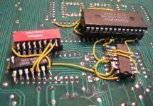
Here's one man's approach to replacing the RAM; kludgy's definitely the word, but hey, it works!
(You should see the ROMs ;-) )

It's a little more complicated than necessary because he provided a switch bank to permit different RAM sizes.

Note that it's installed underneath the board so that it looks normal on top.

I can probably find the schematic in case anyone's actually interested

RAM-1.JPG
 
I'd have to dig through some old stuff, but IIRC it wasn't too difficult to adapt two of Jim Brain's ROM adapters to replace all the RAM and ROM, with an alternate switchable ROM set as a bonus.

http://store.go4retro.com/6540-adapter/

Edit: Turns out I have some of that stuff right in front of me in connection with another project, but it'd take a while to remember/rediscover how it was all connected.

m
 
Last edited:
Back
Top