• Please review our updated Terms and Rules here

3032 - 2001N Repair

I solder temporary wires onto key points on the monitor PCB and then put the dangerous thing back into the case. The other ends of the wires are connected to an insulated "chocolate block" connector so you can attatch probes to them safely.

Can you point me at the schematic for your monitor and I will take a look.

I suspect your IEEE488 BASIC 2/4 issue is down to how BASIC 2 handles a change in state of the ATN input signal. If this line generates an interrupt, some ROM firmware may get in the way in BASIC 2 that doesn't in BASIC 4. That is my educated guess...

Dave
 
Well, there should be +12V on one side of the potentiometer R20 and wiper.

You should also be able to monitor the voltage on the positive side of C9 and the DC level should vary as you adjust the R20 potentiometer.

That would be my first test. The higher value replacement should have no effect with the way R20 is wired.

The schematic (assuming it is the one I have found) seems to have a good selection of oscilloscope traces for various points along the vertical drive circuitry.

Dave
 
The 1M height control sets the charging current in the capacitor C9, this current is when the raster is being scanned, during flyback the capacitor is discharged via the diode and 10k resistor.

One reason the resistance value is so large, its that this helps to create a constant charging current during scan time, not too dependent on the supply voltage. If you imagine a power source with a very high value resistor in series, it acts as a current source.

However, in this case, it does rely on the capacitor C9 behaving as more like an ideal capacitor, in that any electrical leakage can have more of an effect on the circuit and an electrolytic cap in this location was not an ideal choice. If you see a circuit where an electrolytic is charging from a high value resistor, say about 500k with the pot in the middle in this case, then it should ring some alarm bells. In my PET VDU's I changed this part to a 1uF MKT film capacitor to avoid any troubles. Here is the remark from page 11 of my article:

C9 was originally a 1uF 25V electrolytic capacitor. Over the years I have learnt that low uF value electrolytic capacitors are better replaced with a modern film capacitor as they will never likely lose capacitance or suffer physical or electrical leakage issues. Therefore C9 was replaced with a 1uF 63V MKT type in my VDU.

I'm not saying your C9 is definitely faulty, but it is one thing to check.

The circuit you are dealing with, after C9 is basically a DC coupled amplifier to drive the vertical yoke coils. The linearity of the scan is affected by the feedback to the base of the input transistor that C9 feeds. They have applied both negative feedback, for DC Stabilization and to set the working point of this amplifier via R30, and some positive feedback via R27. The positive feedback is the cause of the bounce sometimes seen if there are disturbances in the input Vdrive signal or a bad connection on the height pot wiper.

Obviously the input frequency of the Vdrive signal has to be correct to attain the correct height (because the period determines the time that the capacitor is charging for) so double check that on the scope.

All else being equal though, since the vertical scan is basically working, likely all the transistors are ok, and the suspect parts (assuming the height pot was ok and the +12V supplying it and the resistors/diodes in the area ok) would be the other electrolytics, including C12 and C15, worth checking on the ESR & capacitance meter.
 
Last edited:
OK, need the help of you clever people who understand analog circuits much better than me.
.
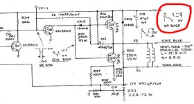
To recap, got a 2001 9-inch monitor, Model 320034 that has a problem with what seems to be the vertical size. This is the relevant part of the circuit (this is 320033, but I've not seen any obvious differences yet):
.
V-Drive Circuit.jpg
.
First order of business was to look at all the electrolytics in this circuit and most of them were measuring significantly higher than specified. The 47uF (C12, C13), read around 60uF, the 470uF measure 550uF, etc. So I replaced them all with new components.
.
C9 read around 1uF but I replaced it with a new one that also measures a lower ESR (~2ohm vs the 6ohm of the one that came out)
.
C10 measures close to the 1nF it should be but C11 measures closer to 1800pF, rather than the 2200pF it should be. I did not replace the two caps as I do not have new ones.
.
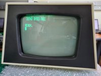
All this made some difference as I now get more of the display than before. Previously just the "Ready" was visible:
20230708_233601.jpg
.
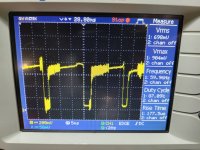
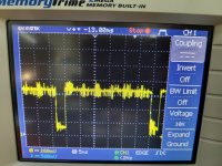
I looked at all the traces and, compared to the provided waveforms, the base of Q8 is the one that's the most out:
.
Q8-base.jpg
.
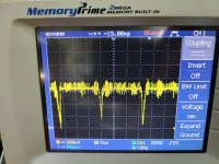
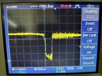
Outside of the noise observed, according to the circuit diagram, the pulse should be 0.2ms but I see closer to 2.5ms. Can this be a factor?
.
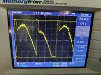
The Collector of Q8 shows the following:
Q8-collector.jpg
.
The signal appears good(ish) but the level is about 12.3V instead of the expected 11.5V.
.
I see the same on the base and emitter of Q9; correct looking wave forms, maybe up to a 1V higher than expected.
.
DC supply is 12.2V with no ripple.
.
Adjusting R20 (Vert Size) makes a very small difference.
.
So, this is where I am, any help and guidance would really be appreciated.
 
Last edited:
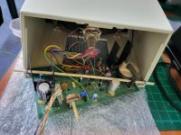
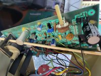
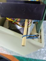
BTW, I ended up securing the PCB in the following way, using a wooden dowel and two elastic bands. This secured the board enough that it does not move and give access to most of the top and bottom of the board. I was going to build a jig to mount the tube and board to give unfettered access to the bottom and the top, but got a bit carried away with the Video Generator project. Maybe tomorrow. :)
.
This is the plastic housing that allows this setup. Clearly, with the metal casing, it would be a different matter.
.
20230708_233523.jpg 20230708_213051.jpg 20230708_213101.jpg
 
Can you post a trace of the base and collector of Q6 please using the same timebase as in post #66 - so we can easily compare the traces.

Dave
 
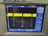
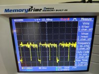
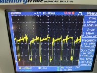
This is V-Drive on the input connector, on the monitor.
The expected pulse width of 1.26ms looks good:
20230709_102129_V-Drive.jpg
.
This is the Base of Q6:
20230709_102303_Q6-Base.jpg
.
This is the Base of Q7:
20230709_102347_Q7-Base.jpg
.
This is the Base of Q8:
20230709_102443_Q8-Base.jpg
 
Was the scope time-base changed between the last two recordings ? Maybe it hadn't and if that was the case, that could be a big clue to the fault.

The recordings also don't make a lot of sense in that each transistor stage is essentially an inverter, for example Q6's base voltage should be approximately anti-phase to Q6's collector voltage (which is Q7's base voltage). And Q7's base voltage should be anti-phase to Q7's collector voltage (which is Q8's base voltage) and this does not seem to be the case from the recordings, are you sure they are correctly labelled ?

To get this sort of pattern (assuming the recordings are correct) it would appear to require a combination of both a defective Q6 and Q7 and both are failing in their role as inverting amplifiers. Q8 is probably ok.
The time-base was the same, I think what happened, is that some of the pulses on Q6 base does not switch the transistor, resulting in the 'missing' pulse on the base of Q7.
Screenshot 2023-07-09 123023.jpg
.
Your point about the transistors not inverting the signal is pretty valid and I should have noticed this. Got me scratching my head now.......
 
Yes, I was confused as well...

Perhaps look at the signals again with this in mind?

You might need a x10 probe on the base of Q6 to avoid loading issues?

Dave
 
I rechecked the signals and they stay the same. Took Q6 and Q7 out and they seem to test OK. They are 2N3903 and I only had 2N3904s (the higher gain version of the 3903), so put new ones in Q6 and Q7.
.
So, thaces below are with 2N3904 in Q6 and Q7.
.
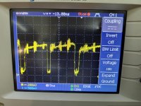
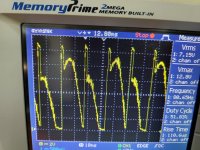
Something that might be relevant is that every second pulse is different. Around Q7, it's evident in the width of the pulse. Around Q8, Q9 and Q10, it translates to a different waveform.
.
This is the base of Q6 (from a previous reading, so the time-base is 5ms. Rest of screenshots are @ 10ms):
20230709_102303_Q6-Base.jpg
.
With a 2N3904, this is the Collector of Q6. notice the width difference of the pulses. Every second pulse is much wider/narrower:
20230709_132901_Q7B.jpg
.
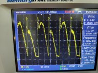
With a 2N3904, this is the Collector of Q8. Same difference in pulse widths.
20230709_133021_Q8B.jpg
.
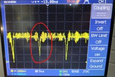
This is the Collector of Q8. Notice the different waveform on every second pulse:
20230709_133123_Q8C.jpg
.
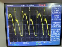
This then appears on Q9 as well:
20230709_133713_Q9B.jpg20230709_133758_Q9E.jpg
.
If I look at the first readings I took (pics higher up #66), I see the same difference on every second pulse.
.
Now I have no idea if this is causing the vertical size issue, but surely these pulse should look identical. Perhaps it's the one with the bigger area under the curve (so to speak) that's overdriving the coils?
 
Yes, I was confused as well...

Perhaps look at the signals again with this in mind?

You might need a x10 probe on the base of Q6 to avoid loading issues?

Dave
I sat now and measured again, see above, am still very confused :)
.
Probe on 10X.
 
If we look at the expected signal on Q9 Base, it should look like this:
V-Drive Circuit-Q9.jpg
.
This matches the lower level pulse actually measured. The other pulses increases in voltage before dropping away.
20230709_133713_Q9B.jpg
.
This must be some timing thing, feels suspiciously like a cap but I've not found any patently faulty caps. C11 measured about 0.0018, rest of them seems to be OK and/or I replaced them.
 
Definitely the pulse width that drives the shape and amplitude of the signal that drives the deflection coils.
.
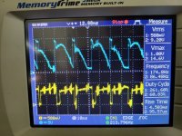
Yellow is Q8 Base and Blue is Q8 Collector.
20230709_144323.jpg
.
Both these pulses are wider than the circuit specifies. It should be 0.2ms but is between 2 and 4ms.
.
Would be great if someone with the same 9" can confirm what they see on Q8 base.
 
Yes, it would be good to get some comparison traces of a working system to compare to.

If the signal on Q6 base is not good, you can forget everything afterwards of course...

Have you checked C10 just out of interest? I guess you have already replaced it?

The other 'annoyance' is the feedback from the circuit containing C14 and C15. I suppose you have checked R32?

I also think you have an entire line missing off the top...

Dave
 
If the signal on Q6 base is not good, you can forget everything afterwards of course...
Indeed. The thing with every second V-drive pulse looking different is telling us something, just no idea what. :) The only bit that seems (potentially) related is in the push-pull output stage. The different width / amplitude pulse things is consistent and there must be a fixed cause for it.
Have you checked C10 just out of interest? I guess you have already replaced it?
It measured OK, but I did not replace it. Will have to get a replacement part. Must it really be a 200V part?
.
C11 is the one that measures quite a bit out, it's reading 0.0018 vs the specified 0.0022. Also need to get a replacement for it.
The other 'annoyance' is the feedback from the circuit containing C14 and C15. I suppose you have checked R32?
This is the thing, right?. I keep on going there. R32 and R28 (2.2ohm) measures correctly in circuit. C14 also measures correctly.
I also think you have an entire line missing off the top...
Not following, which top?
 
Managed to connect another 9" monitor up and do some measurements around Q6, 7 and 8. Board is still in the casing, so a bit difficult to measure.
.
The signals are significantly different.
.
Q6:
In the faulty monitor, there are significant levels around Q6, with a 3V pulse on the base and 600mv on it's collector.
On the working monitor, I literally cannot measure the signals around Q6. It's within the noise floor of my test setup and probably how I connected it to the monitor.
.
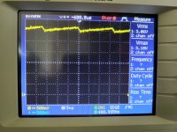
C9:
On the working monitor, I get this signal on the positive side of C9:
20230709_171024.jpg
.
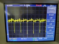
Q8 base:
On the working monitor, I get the expected signal on the base of Q8. ~0.5ms and 0.7V. The circuit says 0.2ms.
On the faulty monitor, this pulse is up to 5ms.
20230709_170436.jpg 20230709_170507.jpg
.
Q8 Collector also looks good and the different shape 2nd pulse is not seen. All the pulses look like the waveform on the circuit.
.
It's like V-Drive is being applied nearly directly to the base of Q6 and over-driving everything. Nearly as if C9 is shorted. I've replaced C9 (twice) but I'm now going to look if there's not a short on the board around the input components (CR8, CR12, R15, C9). I've tested all of them already but I've not looked for a potential short, open-circuit or other issue on the board itself.
.
Any other suggestions will be helpful.
 
Self help is always good!

>>> It measured OK, but I did not replace it. Will have to get a replacement part. Must it really be a 200V part?

No, but it is a moot point now isn't it.

>>> Not following, which top?

There is the "*** COMMODORE BASIC ***" message missing from the top line of the monitor...

I think what you are seeing on the positive side of C9 is correct. C9 charges up via R20 and R21 and discharges via CR8, CR12 and R15. There should be no 'pulse' on here (if things are working correctly of course).

The problem with BJT transistors is that they amplify CURRENT - so looking at the voltage (especially on the base of a transistor) doesn't actually tell you too much...

Is it possible that C9 has been previously replaced by someone else for an incorrect device and you have replaced it for an equivalent (but still incorrect) device? Perhaps replace it with what Hugo recommended?

As Hugo also mentioned, R30 sets the operating point of Q6 and R27 sets the amount of feedback. Something wrong with either of these components (or somewhere from Q6 through to the feedback path - Dooo) would also cause problems.

I think you will find (and Hugo will correct me here) that Q6 is 'just' biased at the correct operating point and then the small current change in Q6 base causes a large 'switch' at the output of Q7 collector.

Dave
 
Last edited:
Back
Top