NobodyIsHere
Veteran Member
- Joined
- Dec 20, 2006
- Messages
- 2,412
Hi! I need a list of the latest discoveries on the prototype for the respin. What I have so far is:
1. mounting holes for the bracket
2. move the indicator LED
3. write enable jumper for the EEPROM
There was an other list of items for the respin earlier in this thread which I've already implemented so these are the new and/or remaining issues.
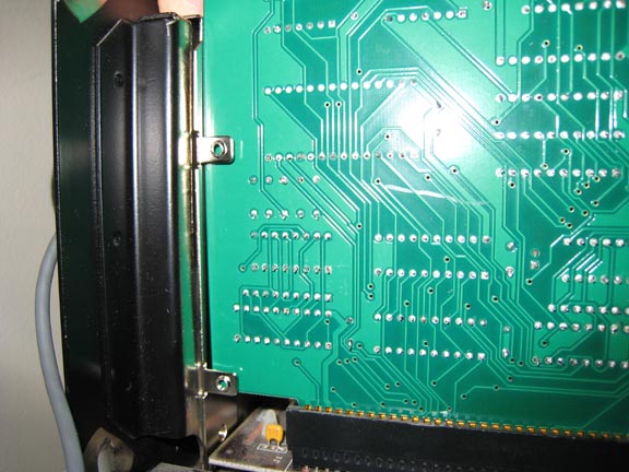
As for the new prototype PCB, I've noticed it seems a bit more responsive than the wire wrap prototype as well. I can't prove it but the new prototype just seems "crisper" and things are moving more quickly. That's not unusual though, I've often noticed that I can get prototypes to work but when moved to a PCB the design just seems to respond better and more reliably.
It may be partially just a perception but there is probably some truth to it. The PCB has much shorter leads and more direct traces that are probably lower impedance. I suspect the wire wrap prototypes add in a bunch of noise due to RLC effects of all the wires. That Hargle noticed that some drives now perform better than before seems pretty compelling that something has changed for the better. That's good.
So things are moving along in a positive direction. I have only one remaining question though... what happened to the first PCB prototype? What I'd do is print off the schematic and PCB layout from the wiki and use the VOM to do a connection by connection wring out, marking each connection as you go. Also, use a bright light and a magnifying glass to inspect each of the solder joints for misses, cold solders, bridges, etc. Go over the board again and remelt all the joints with your soldering iron to wipe out any cold joints and remove any excess solder. Check each IC for bent or wrapped under pins in the socket.
You can also use the VOM to find hidden bridges by inspecting continuity between pins and comparing to the schematic. Failing all of those, leave the working prototype PCB board alone and get some more ICs and do a chip swap to isolate the broken part. If the ROM still does not appear in the memory map, the problem has to be in or near U9, U10, RR2, or SW2 since it is basically a separate subsystem.
If you've got a logic probe check to see if U9 is generating the chip select pulse when you access the ROM in the memory. That'd be U9 pin 19 or U10 pin 20. You can always send it to me and I'll beat on it for while but you're right that you're going to need to debug these things when the project moves to a production phase as issues found in assembly is normal.
Thanks and have a nice day!
Andrew Lynch
1. mounting holes for the bracket
2. move the indicator LED
3. write enable jumper for the EEPROM
There was an other list of items for the respin earlier in this thread which I've already implemented so these are the new and/or remaining issues.
As for the new prototype PCB, I've noticed it seems a bit more responsive than the wire wrap prototype as well. I can't prove it but the new prototype just seems "crisper" and things are moving more quickly. That's not unusual though, I've often noticed that I can get prototypes to work but when moved to a PCB the design just seems to respond better and more reliably.
It may be partially just a perception but there is probably some truth to it. The PCB has much shorter leads and more direct traces that are probably lower impedance. I suspect the wire wrap prototypes add in a bunch of noise due to RLC effects of all the wires. That Hargle noticed that some drives now perform better than before seems pretty compelling that something has changed for the better. That's good.
So things are moving along in a positive direction. I have only one remaining question though... what happened to the first PCB prototype? What I'd do is print off the schematic and PCB layout from the wiki and use the VOM to do a connection by connection wring out, marking each connection as you go. Also, use a bright light and a magnifying glass to inspect each of the solder joints for misses, cold solders, bridges, etc. Go over the board again and remelt all the joints with your soldering iron to wipe out any cold joints and remove any excess solder. Check each IC for bent or wrapped under pins in the socket.
You can also use the VOM to find hidden bridges by inspecting continuity between pins and comparing to the schematic. Failing all of those, leave the working prototype PCB board alone and get some more ICs and do a chip swap to isolate the broken part. If the ROM still does not appear in the memory map, the problem has to be in or near U9, U10, RR2, or SW2 since it is basically a separate subsystem.
If you've got a logic probe check to see if U9 is generating the chip select pulse when you access the ROM in the memory. That'd be U9 pin 19 or U10 pin 20. You can always send it to me and I'll beat on it for while but you're right that you're going to need to debug these things when the project moves to a production phase as issues found in assembly is normal.
Thanks and have a nice day!
Andrew Lynch
")
