• Please review our updated Terms and Rules here

Build your own PDP 8I, Part 3..

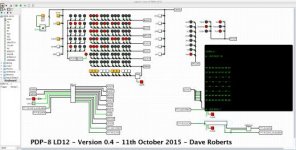
I have just got my TTY hooked up in LOGISIM - the simulation now runs MAINDEC-8I-D02B as well now.

The sample programs for the LD12 TTY do not appear to work. The "Echo program" has a line missing from the bottom of it (i.e. add 0007 5000 JMP 0) and I don't believe that the "Print all possible characters" program works at all.

I will do a bit more testing this week with the MAINDEC-8I diagnostics to see if anything else is revealed before publishing the next version. I have managed to start playing Chess (CHEKMO-II) - but for some reason it is taking a very long time to make its move. This could be due to a 'bug' in my LD12 logic (more testing and checking required on my part) or it is just too slow to run in the LOGISIM environment (I need to make a hardware implementation like Marty!).

I can, however, confirm that signal A0 is *** NOT *** required to be wired up to gate E4/A37 pin 4 in the production of PC(L). This causes the PC to be incremented as part of the interrupt handling process with the result that the return address that is stored is one more than it should be. D02B identified this 'undesirable feature'. Interestingly, it is identical to the bug I had when I did the LD30 microcoded unit...

Dave
 
Hi All;

Dave, Great Progress !!!!
"" I can, however, confirm that signal A0 is *** NOT *** required to be wired up to gate E4/A37 pin 4 in the production of PC(L). This causes the PC to be incremented as part of the interrupt handling process with the result that the return address that is stored is one more than it should be. D02B identified this 'undesirable feature'. ""
Great, I will make the Change permanent in the Schematic..

THANK YOU Marty
 
Hi All;

I have mostly wired up LD-8 through LD-11..
I say mostly, as there are some things that are not wired, since where they connect is not wired, a later LD-nn..

001.jpg


THANK YOU Marty
 
Last edited:
Hi All;

Dave, I found that using Logisim, I could view the Schematic, and quite easily.. I didn't know that before..
So, I have copied Your Clock Schematic and will wire it next..
Also, I found (with a note by You) the the second half of L8 and L9 are wired backward from my Schematic.. Correct ???
And so I need to change my Schematics ??
Are there any other places that need to have changes made to them ?????

THANK YOU Marty
 
I have now run Version 0.4 of my PDP-8 LD12 LOGISIM simulation (dated 11th October 2015) with the following MAINDEC-8I diagnostics and they run fine:

D01B
D02B
D04B
D05B
D07B
D11A @ address 0000
D11A @ address 7400

And I have also run it with CHEKMO-II (although it runs rather slooooooowly under the software simulator).

See attached files (image of LOGISIM with the 'front panel' running CHEKMO-II and a ZIP of the LOGISIM circuit file).

Enjoy!

Dave
 

Attachments

  • PDP8_LD12_MAIN_CHEKMO-II.jpg
    PDP8_LD12_MAIN_CHEKMO-II.jpg
    29.3 KB · Views: 7
  • PDP8-LD12.circ.zip
    51.3 KB · Views: 4
Marty,

Ah - so you have managed to get LOGISIM running enough to see the schematics. Great news.

On the top-left is a vertical list of all of the individual schematics. MAIN is obviously the front panel (!) with PDP having most of the PDP-8 LD20 logic on it. The other key modules are the individual registers (e.g. MA, PC and AC) - generally constructed from software simulations of the TTL chips themselves (so you should be able to see the 'pinouts' of the chips I have used corresponding to the SN74XX devices).

There are a couple of 'logical' blocks (e.g. EAGEN) (standing for Effective Address GENeration) which encompass the necessary gates to implement that function without 'cluttering' the main schematic with logic. This makes it easy to add something like the EAGEN, AMUX and ALU in series on the PDP schematic without a load of gates confusing the issue.

Note, however, that I have taken a few short-cuts. For example, a SN7474 has an active low set and clear - but the default D-type flip-flop in LOGISIM has an active high set and clear. I couldn't be bothered to make up my own 7474 D flip-flop with the correct 'sense' of the set and clear inputs so I have added 'imaginary' inverters to my schematic. These should be obvious, as I have added (DER) after the IC reference.

Select the little 'hand' symbol on the top left of the menu bar and then try and open the ALU schematic by double clicking on the centre of it - do three 74181 IC's appear? If they do - double-click in the centre of one of the 74181 devices - and the schematic diagram should open of the logic within the device itself. This test is good - because it shows that the libraries are working as expected. if not - I can guide you through installing the 74-series libraries that you require.

You should then be able to run the simulation by selecting the menu options Simulate->Simulation Enable (select a tick next to it) then Simulate ->Ticks Enabled (again, select a tick next to it) and finally Simulate->Tick Frequency->4.1 KHz to make it run ‘fast’ (but not as fast as your hardware implementation though!).

You should see random simulated LEDs flash on the front panel if all is well. Press the yellow STOP button followed by the yellow CLR button. The RUN, FETCH and EXECUTE LEDs should go out.

You should now be able to set values up on the switch register (SWRIN), store the value in MA or PC, use EXAM or DEP to store/read data into/from memory and CONT to execute an entered program. If you can get this far - I will tell you how to load programs (such as the MAINDEC-8I diagnostics) straight into the memory of the simulation from a file.

The part about the second half of L9 and L8 is that we are both right(!). If you read the Lab Manual (bottom of page 99) you will see what I am talking about. Pin 13 of L9 is drawn as J but with an inversion circle. If you check the EXT-sorted wiring list for L9; pin 13 is identified as ‘K2-“. So how come pin 13 of L9 can be both J and K simultaneously? Is it a fault? Well, no. The critical thing is the circle on the schematic that gives it away. A 9024 flip flop has J and /K inputs to it. Whereas the schematic is drawn as /J and K.

This is a similar issue to drawing an SN7400 quad NAND gate package as an OR gate with inverted inputs. It is counterintuitive - but logically correct by DeMorgan’s Theorem. All that the guy has done when drawing the schematic is to refer to how the gate is used ‘logically’ (with the J input being inverted and the K input not). I just saw the J and K inputs for L9(2) and wired them up as the J input to ‘1’ and the K input from G9/12 on my LOGISIM schematic. This is incorrect as the ‘1’ is connected to pin 13 of the IC (which is really the /K input), and G9/12 is connected to pin 14 of the IC (which is really J). Simples!!!

Marty, the LD12 wiring is physically correct for these two gates - so don’t worry too much about it if the explanation in the Lab manual or my poor attempt above doesn’t make any sense.

Incidentally, (to compound your headache), LOGISIM implements a JK flip-flop as a J and K input (not a J and /K input as per a real 9024). I had, therefore, to invert the K input signal before passing it to the LOGISIM equivalent flip-flop (hence the (DER) inverter on all the K inputs - and the Set and Clear inputs as well).

I hope that explanation is clear…

Dave
 
Hi All;

Dave, Thank You for the lengthy summary, Yes, I need to know about Loading the correct Library files and in what Order.. OtherWise the rest is alright..
"" Note, however, that I have taken a few short-cuts. For example, a SN7474 has an active low set and clear - but the default D-type flip-flop in LOGISIM has an active high set and clear. I couldn't be bothered to make up my own 7474 D flip-flop with the correct 'sense' of the set and clear inputs so I have added 'imaginary' inverters to my schematic. These should be obvious, as I have added (DER) after the IC reference. "" "" Incidentally, (to compound your headache), LOGISIM implements a JK flip-flop as a J and K input (not a J and /K input as per a real 9024). I had, therefore, to invert the K input signal before passing it to the LOGISIM equivalent flip-flop (hence the (DER) inverter on all the K inputs - and the Set and Clear inputs as well). ""
Yes, I saw these and Your Explanation helps alot..
Even though I will probably have to re-read the section on the 9024's to make sure I understand it correctly..
I have switch pins 13 and 14 on the two L8 and L9..
Dave, Can You TRY something for me, It will (I hope) clear another thing up..
On E15 pin 1 is hooked up to F1, Try hooking it up instead to F0, and RE-Run all of the Tests, and Let me know what the Diagnostics say, Maybe they will say that F0 is more correct or maybe not.. And we will not be any better or any worse..
I finally got out my scope and the frequency I was running was about 90hz, and now it's about 40 hz while in debug mode.. So, it's actually running about half of that at present or somewhere in the 15 to 20 hz range..
THANK YOU Marty
 
Last edited:
Just to confirm, the existing LD12 schematics ARE CORRECT for the pinouts of L8 and L9 (2nd half flip-flops).

I will make the change you want me to try tomorrow - it is bed time in the UK!

I noticed I had put a comment next to this pin on my LOGISIM drawing - but hadn't gone back to it. I notice that for the LD12 there are two schematics (one showing F0 and the other showing F1 connected to this pin). Both can't be right! It is my belief (although I will prove it tomorrow) that neither of them are actually required for correct operation - although it will influence what is stored into the MB register at one of those fetch states (i.e. it is a front panel 'correctness' issue rather than functional). As I understand it, the original PDP8 used the MB register to interface to and from the memory - however (in the LD12) there is an M input to the large MUX. This is not the same as using the MB register - so an extra step is required to store the M value in MB.

Just a thought.

Dave
 
Hi All;

Dave, Thank You for Your response..
"" It is my belief (although I will prove it tomorrow) that neither of them are actually required for correct operation. ""
Yes, go ahead and check F0, F1 and nothing..
"" however (in the LD12) there is an M input to the large MUX. This is not the same as using the MB register - so an extra step is required to store the M value in MB. ""
I would be interested in it's results..
I had to go and Look, M is Memory out, and MB is Memory in, On the 7489's..
Also, it look's like I will need to wire up the Registers and the ALU and the associated items, to be able to check out the next stage..
Which is exactly where I was before in my last wiring..
I am confused, on L8, so just to set me straight is VCC connected to pin 13 or pin 14, I can figure out L9, once I have L8 straightened out..
I have taken two pictures, the first is my slightly modified Clock circuit, from Dave's Clock circuit.. The second is what I have added of Ic's since last picture.. Except for the clock circuit, I have added no other circuitry (wires)..

001.jpg 002.jpg

THANK YOU Marty
 
Last edited:
Dave & Marty,

Outstanding work, Gentlemen!

Thanks for sharing & thanks to those who provided the original LD12 material and a place to post it so this could happen.
 
That looks very pretty Marty!

Thanks for the 'thumbs up' DDS. I am doing the easy bit (pushing a mouse around), Marty is cutting has hands on all those wire wrapping pins and has the hard job!

Marty: Vcc is connected to pin 13 on chip L9(2) of schematic LD 9 exactly as mark Arnold's schematics show. Hope that is now clear for you?

I have done a quick and dirty test this evening with E15 pin 1 as you suggested. I have run a couple of passes of diagnostics D01B and D02B. I get the same results (a PASS) whether F0, F1 or logic '1' (Vcc) is connected to E15 pin 1 - thus proving my understanding that none of these signals are significant to load the MB register at this stage.

However, I am just chasing down another anomaly with the logical expressions fed to pins 4 and 22 of IC J7. These logical expressions also differ from the state diagram descriptions. I think I may have to work these out from first principles though.

I will run another exhaustive diagnostic test over the weekend again with E15 pin 1 connected to Vcc. Last Sunday I ran all of the diagnostics over a 9 hour period!

I now need to start ordering my chips to make one now!

Dave
 
Almost forgot,

There is another slight problem I tripped over with the LD12 as it stands.

On power-up most of the flip-flops contain a random state. The STOP and CLEAR button only resets some of them. This statement is also applicable to the TTY interface.

Just a note of caution...

Dave
 
Hi All;

Dave, Thank You for the Heads up.. "" Vcc is connected to pin 13 on chip L9(2) of schematic LD 9 exactly as mark Arnold's schematics show. ""
Yes, it clears it up, the reading of everything, got me confused..

"" That looks very pretty Marty! "" Thank You Dave and Thank You DDS for Your encouraging words..
"" Marty is cutting has hands on all those wire wrapping pins and has the hard job! ""
Actually, it is not very hard at all, its more time consuming and can get boring and hard on the eyes..

"" I have done a quick and dirty test this evening with E15 pin 1 as you suggested. I have run a couple of passes of diagnostics D01B and D02B. I get the same results (a PASS) whether F0, F1 or logic '1' (Vcc) is connected to E15 pin 1 - thus proving my understanding that none of these signals are significant to load the MB register at this stage. ""
For now I will tie it to the pin next to it, that makes it easy to change if needed..

"" However, I am just chasing down another anomaly with the logical expressions fed to pins 4 and 22 of IC J7. These logical expressions also differ from the state diagram descriptions. I think I may have to work these out from first principles though. ""
Yes, I would like to know more.. I will see If I can find the expressions and do the same.. I am not saying that I can do this, but it would be good experience for me..

"" On power-up most of the flip-flops contain a random state. The STOP and CLEAR button only resets some of them. This statement is also applicable to the TTY interface. ""
I knew about this, and for now I choose to leave it this way, that way by clearing each register, individually, I would know that my LoaDing of the register was actually working.. Once I am sure of things working, then I will implement Clearing all of the Registers with the push of one Button..

THANK YOU Marty
 
Hi All;

Dave, "" However, I am just chasing down another anomaly with the logical expressions fed to pins 4 and 22 of IC J7. These logical expressions also differ from the state diagram descriptions. I think I may have to work these out from first principles though. ""
Have You had the time or had any luck at doing this ??
Dave, while You are at it, can You try another Variation out for me..
On LD21, it has K19 pin 1 tied to IR11, and K19 pins 2 and 4 tied to IR3-8 inverse and K19 pins 5 and 13 tied to IOT.h (K18.6)..
K19.3 is tied to IR11 inverse in my schematic on one version and tied to IR10 in another version..
Can You check which is Correct or more Correct or if one fails.. THANK YOU..

I have wired up all of the Register and Accumulator inputs.. I also, just realized I made a mistake in my initial planning, and so I will need to wire up three of my 16 pin sockets for 14 pin 7404's.. No other place to put them, that is near where they are needed.. Which is also why I provided and planned for extra Blank sockets..
I have also found that my thinking was wrong, when I thought I would use 74175's instead of 74174's, and use the inverted outputs to drive the Led's.. But now to do that I would need to use many more sockets, either for extra R-Pack if I used 7407/7417's for the Led Drivers, or add another 7404 gate ahead of the Led Drivers.. But, since I have wired the 74175's into the circuit, I will use them for the most part as 74174's on the non-inverting outputs.. My Initial idea was to not have as many loads on the 74175's as I did on the 74174's by using inverted and non-inverted to share the Loads..
Next, I will wire up the Accumulator and the Link Bit, as well as it's Led's..

001.jpg 002.jpg 003.jpg

THANK YOU Marty
 
Last edited:
I haven't fully got to the bottom of the anomalous equation - although I am getting there.

The expression fro NOMEM in the second edition of the book is "NOMEM = OP+IOT+DIRECT*(DCA+JMS+JMP)" where DIRECT = /IR3. This is what I used in my microcoded LD30 and it works as expected. In the second edition of the book (for the non-microcoded LD20) - it uses the same expression. Hence the reason I am a little confused over why JMP is singled out for special treatment in the LD12 but not DCA or JMS. The drawings we have for the LD12 FETCH state diagram also shows the same logical expression. These are classed as "Early exits to Execute" - so it may be that if you leave them out they don't do any harm (it just takes the FETCH process longer for no reason). I will continue to look and see if they have any unforeseen side effects though (although the MAINDECs run OK without them).

I did 'fall over' another problem - which also didn't seem to be detected by the MAINDECs. I noticed that PC is used in the computation of the Effective Address (EA) for the PAGE bits. In my microcoded LD30 design - this was the MA register not the PC. I thought it a bit strange when I changed this in my LD12 LOGISIM drawing (meaning to come back to it later). Well, later is now. I have just toggled in a simple program and it doesn't seem to work as expected. The PAGE bits are supposed to be taken from the PC of the EXECUTING instruction. The MA register is loaded with PC and the current instruction fetched from memory to IR. After this the PC is incremented and then any EA calculated if necessary. At this stage, the PC has already been incremented. This won't make any difference UNLESS the instruction that was executed is on a PAGE boundary (e.g. address 0177). The PC would wrap-over to 0200 after the current instruction was fetched and (say) A DCA to the current page would store the result in page 1 instead of page 0. I thing MA should, therefore, be used in preference to PC in the determination of EA.

STOP PRESS - I have just checked out the two sets of schematics I have and they are different in this area! In one set, PC is used for the EA page number. In the other set, MB is used for the EA page number. Neither uses MA! Does this now account why F0 is used to load MB from PC in state F0? PC is transferred to both MA and MB in state F0. MA is used to address memory and the result stored in IR in state F1. The PC is incremented in state F2. State F3 calculates the EA and reads the operand. EA uses the value of MB for it's 'old PC'. If EA used MA rather than MB then F0 would not need to store the PC into MB (simples!)

The issue regarding the use of IR10 or IR11 for determination of ION and IOF is that they are probably both right depending upon your view!

An ION instruction is encoded as 6001 and an IOF instruction is encoded as 6002. The logic decodes for 600x (which is correct for an ION/IOF instruction). However, the bits to decode IR11, IR10 and IR9 are a bit indeterminate. You could use IR11 to decode the two instructions (1=ION 0=IOF) or you could use IR10 (0=ION 1=IOF). It was up to the student (presumably) how they decided to do it... One chose IR10, another IR11. Yet another may have chosen to incorporate IR9=0 as well?

Dave
 
Hi All;

Dave, Thank You for the informative reply.. Keep UP the GOOD/GREAT Work !!

"" The expression fro NOMEM in the second edition of the book is "NOMEM = OP+IOT+DIRECT*(DCA+JMS+JMP)" where DIRECT = /IR3. This is what I used in my microcoded LD30 and it works as expected. In the second edition of the book (for the non-microcoded LD20) - it uses the same expression. Hence the reason I am a little confused over why JMP is singled out for special treatment in the LD12 but not DCA or JMS. The drawings we have for the LD12 FETCH state diagram also shows the same logical expression. These are classed as "Early exits to Execute" - so it may be that if you leave them out they don't do any harm (it just takes the FETCH process longer for no reason). I will continue to look and see if they have any unforeseen side effects though (although the MAINDECs run OK without them). ""

I would try The Equation that You have had success with, and If it works in this Version, then I would say Let's go with it ..
I will look it up and I can try and wire it, but I am NOT sure where it is implemented and Where it is attached in the circuit..
Once I see how You have it plugged in, I will go, OK, that was easy..
The Reason I am asking is that in Your stated questioning on two states, (If I remember correctly pin 4 and pin 22, so which one pertains to Your above description or is it both ?
I went to the Book and Found NOMEN and so I got the answer to my Question, it is F3..
Also, OP is what we call MIC, So now I know where to start, in looking for sameness and differences..
I found the Schematic, so it would be easy to implement, just take out K16, pins 8 and 9 (the 7404) and insert a 7410 for JMP+JMS+DCA..
Dave once, you have Determined that this works with this version, I will change my Schematics..

"" STOP PRESS - I have just checked out the two sets of schematics I have and they are different in this area! In one set, PC is used for the EA page number. In the other set, MB is used for the EA page number. Neither uses MA! Does this now account why F0 is used to load MB from PC in state F0? PC is transferred to both MA and MB in state F0. MA is used to address memory and the result stored in IR in state F1. The PC is incremented in state F2. State F3 calculates the EA and reads the operand. EA uses the value of MB for it's 'old PC'. If EA used MA rather than MB then F0 would not need to store the PC into MB (simples!) ""

I had tried that and wired MB and it Did Not Work..
However, I do need to Re-Read Both of Your Paragraphs and TRY to Understand them, it is Not Your Explanation, but, my Understanding..

"" The issue regarding the use of IR10 or IR11 for determination of ION and IOF is that they are probably both right depending upon your view!
An ION instruction is encoded as 6001 and an IOF instruction is encoded as 6002. The logic decodes for 600x (which is correct for an ION/IOF instruction). However, the bits to decode IR11, IR10 and IR9 are a bit indeterminate. You could use IR11 to decode the two instructions (1=ION 0=IOF) or you could use IR10 (0=ION 1=IOF). It was up to the student (presumably) how they decided to do it... One chose IR10, another IR11. Yet another may have chosen to incorporate IR9=0 as well? ""

OK, So I will not worry about it..

THANK YOU Marty
 
Last edited:
If you had used MB in the EA logic ( drawing LD18 ) then signal F0 would have to have been included to E15 pin 1 on drawing LD15 to load the MB register at time F0.

If I remember correctly, you had F1 wired to E15 pin 1 at some point (as per the 'other' set of drawings that used PC in determination of EA).

If you had used MB in the determination of the PAGE for EA - but wired F1 to E15 pin 1 - this would have inadvertently used the top 5 bits of the instruction itself (opcode + I + Z bits) as the PAGE - with somewhat disastrous consequences!

This project is better than reading a murder mystery!

My proposal is to use MA in the determination of EA and to wire E15 pin 1 back to E15 pin 2 (i.e. unused).

Dave
 
Hi All;

Dave, Thank You for the answer..
"" If you had used MB in the EA logic ( drawing LD18 ) then signal F0 would have to have been included to E15 pin 1 on drawing LD15 to load the MB register at time F0.
If I remember correctly, you had F1 wired to E15 pin 1 at some point (as per the 'other' set of drawings that used PC in determination of EA).
If you had used MB in the determination of the PAGE for EA - but wired F1 to E15 pin 1 - this would have inadvertently used the top 5 bits of the instruction itself (opcode + I + Z bits) as the PAGE - with somewhat disastrous consequences! ""

I don't remember whether I used F0 or F1 with MB.. And the same goes for the IR bits..

So, I will try it with the MA bits and do as You say.. Fortunately this can be easily changed, I did it before..
"" My proposal is to use MA in the determination of EA and to wire E15 pin 1 back to E15 pin 2 (i.e. unused). "" Thus Eliminating F0..
"" This project is better than reading a murder mystery! ""
Maybe we should write a Book on it.. Even though You are doing Most of the Work..

THANK YOU Marty
 
Last edited:
Marty,

We are writing a book on it already - we just have to extract the ten parts (!) of the posts from VCF and edit them :)

As I said before - I am just wielding a mouse within LOGISIM. You are turning it into a reality in hardware - although I am about to place my order for most of the chips to start making mine. Thanks for the 'heads-up' on the prototyping board though. I eventually located something suitable at Mouser.

Dave
 
Hi All;

Dave, Thanks for the Great Postings..

"" We are writing a book on it already - we just have to extract the ten parts (!) of the posts from VCF and edit them ""
Hadn't thought of that..
"" Thanks for the 'heads-up' on the prototyping board though. I eventually located something suitable at Mouser. ""
I hope what ever You get is large enough..
I won't say which place is best for Your Ic's..
Also, If You can afford it, I would also suggest Machine Wire-Wrap Sockets.. and Plenty of Led's..
Also allow Extra 7404's for the Led Drivers.. They work fine, in place of 7405's or 7406's etc..
In the Last few days, I have wired up the AC(L) circuit, the AC Link Circuit, the CMA circuit, the CLA Circuit, the CLL Circuit and the RAL and RAR Circuits..
Next is the Led's for the Accumulator, and the Rest of the ALU and the Multiplexers for the AC and Data Switches..
Then I can Test the Accumulator !!
The Mux is wired, but the control for the Mux is not wired.. The ALU is wired..
So, all that is left is the Data Switches, the Led's, the Carry in and out, and control for the Mux (B1, B2, B4)..
The Control is next, then the Carries, then the Led's and last the Switches, there are wires on the Switches, they just are not wired..

001.jpg

THANK YOU Marty
 
Last edited:
Back
Top