• Please review our updated Terms and Rules here

CBM3032 garbage screen (yes, another one...)

Papalapa

Experienced Member
Joined
Mar 5, 2024
Messages
72
Location
Barcelona
Today it's a sad day for me, my CBM3032 shows a garbage screen and do not turns on :cry:. I have to say that I'm not a technician, this is just a hobby for me and therefore I don't have oscilloscope, just a digital multimeter and a cheap logic probe. After reading lots of posts in the forum what I have done until now is:

1) Checked voltage transformer outputs and all of them are correct as follows:
pins 4 and 5: 8,7v
pins 4 and 6: 17,4v
pins 5 and 6: 8,7v
pins 7 and 8: 16,6v
pins 9 and 10: 17v

2) Checked DC voltages in the PCB and all of them are correct as follows:
CR10 and CR11 anode: +4,9v DC
CR12 anode: +12,2v DC
CR13 anode: -5,0v DC

3) Measured the 6502 pins with the logic probe with the following results:
Pin 38 (SO): 1
Pin 2 (RDY): 1
Pin 6 (/NMI): 1
Pin 4 (/IRQ): 1
Pin 40 (/RESET): 0 at the startup and 1 after 1 second.
Pin 37: (PHIO): 0+1+PULSE in the probe turned ON
Pin 39 (PHI2): 0+1+PULSE in the probe turned ON
Pin 7 (SYNC): 0+1+PULSE in the probe turned ON

4) Released UC5, UC6 and UC7 and the garbage screen remains.

5) Set the Dave's PET TESTER chip in UD8 and the garbage screen remains.

6) Replaced 6502 by a good-one working in another board.


As far as I know, if the 6502 and the Kernal ROM are OK, the PET tester should start it isn't?

What else can I try?

Thank you
 
With pulsing on 6502 CPU pin 7 this indicates that the CPU is actually executing instructions (somewhere).

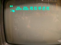
One man's garbage screen is not the same as another man's garbage screen. So, before we disappear down a rabbit hole, can you post a photograph of the screen after you turn the PET on? For now, leave UC5, UC6 and UC7 out and my PETTESTER ROM in UD8.

With UC4 pin 7 pulsing, can you check pins 1 through 24 of UD2 please, reporting HIGH, LOW or PULSING against each pin number.

This will tell me what the 6502 CPU is accessing.

Dave
 
Thank you for your quick response. Here's the requested data:

UC4 pin 7: Pulsing

UD2 pin 1: 1
UD2 pin 2: 1
UD2 pin 3: 1
UD2 pin 4: 1
UD2 pin 5: 1
UD2 pin 6: 1
UD2 pin 7: 1
UD2 pin 8: 1
UD2 pin 9: 0+1+PULSE
UD2 pin 10: 1
UD2 pin 11: 1
UD2 pin 12: 0
UD2 pin 13: 1
UD2 pin 14: 1
UD2 pin 15: 1
UD2 pin 16: 0+1+PULSE
UD2 pin 17: 1
UD2 pin 18: 0
UD2 pin 19: 0
UD2 pin 20: 1
UD2 pin 21: 0+1+PULSE
UD2 pin 22: 1
UD2 pin 23: 0
UD2 pin 24: 1

And here's also the garbage screen video because in this way you'll able to see the small artifacts between the characters:

View attachment IMG_4767.MOV
 
That is roughly what I expected to see.

The display is truly the 'random' display that usually indicates the power-up state of the video RAM.

Pin 9 pulsing (/SEL8) indicates that something is trying to access the video RAM.
Pin 16 pulsing (/SELE) indicates that the PETTESTER ROM is being accessed.

No other output is being decoded from UD2 - so it is running the PETTESTER ROM and PETTESTER seems to be trying its best to write to the video RAM. But, for some reason, the video RAM writes are not working.

Inputs A, B, C and D, on UD2 pins 23, 22, 22 and 21 (respectively) are not wholly consistent - but we are using a logic probe (and this is not the best tool to see narrow pulses).

Next points to look at are:

A5 pin 8. This signal (/TV READ) should go LOW when PETTESTER is trying to read from the video RAM.
A5 pin 12. This signal should go LOW when PETTESTER is trying to write to the video RAM.
F6 pin 7. This signal (TV RAM R/W) is a qualified read/write signal to the actual video RAM. It should go LOW on a video RAM write.

Again, HIGH, LOW, PULSING.

We may be starting to get into territory where the logic probe may not be an adequate test tool - but let's see how things go.

Dave
 
Thank you for your time Dave.

According to my CBM3032 diagrams (remember, I'm not technician :)) when do you say "A5" I guess that do you refer to UG7 (74LS10), and when do you say "F6" I guess that do you refer to UH4 (74LS157). If so, in the three proposed pins to check I get a 0+1+PULSE in my probe.

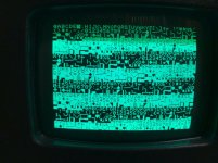
On the other hand, I don't know how but after closing the cover with the monitor this screen from the PETTEST was shown:

IMG_4770.JPG

As you can see there are a few wrong characters, and the test stuck at this point. I turned the PET OFF and ON several times but I have not seen the test screen anymore.

I have forgotten to say that I released all the ICs and applied Contact Cleaner in the sockets. I also checked the three screws that fix the PCB to the metallic base and all of them are properly tighted.
 
When I say A5 I mean UA5 (74LS10) and when I say F6 I mean UF6 (74LS157).

You appear to have (somehow) picked two other ICs with the same part numbers as the parts you should have been probing.

Just to confirm, what is the number stamped on the PCB? It should be something like 320350.

I suspect that the odd character display error is down to a faulty video RAM (UF7 and/or UF8).

However, if you can't get the PETTESTER screen to display again, I would avoid changing anything.

Do you still get the random screen display still on the PET? If so, repeat the tests above (let's make sure we have pulses on UD2 pins 9 and 16, and then move on to the correct IC pins I specified (UA5 pin 8, UA5 pin 12 and UF6 pin 7)).

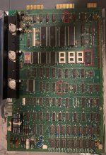
Can you also post a photograph of the logic board and identify which ICs are in sockets. If it worked once, it may be a bad connection. Also, what colour are the IC sockets? It sounds a bit of a daft question, but certain coloured sockets can sometimes be intermittently faulty.

Dave
 
Here we go again...

I'm sorry, you were right. I connected the probe to UH4 instead of UF6 (same IC type). The s/n stamped on the PCB is 33011919. After repeting the readings three times I got the same results as follows:

UA5 pin 8: 0+1+PULSE
UA5 pin 12: 1
UF6 pin 7: 1
UD2 pin 9: 0+1+PULSE
UD2 pin 16: 0+1+PULSE

The garbage screen is random, but only some characters are different from the video shown in my video of post #3. The patterns are very very similar.

Here's the requested picture. You can see the ICs where I measured and the ICs that are socketed. The sockets are all of them white color.

IMG_4643.JPG
 
>>> The s/n stamped on the PCB is 33011919.

That is the serial number, not the part number. It is the part number that defines what version of the board you have - but it is going to be a 2001N with a part number of 320348, 49 or 50. It may be on the solder side of the PCB. I don't think we need it now we have identified the correct ICs to probe...

>>> The garbage screen is random, but only some characters are different from the video shown in my video of post #3. The patterns are very very similar.

Static RAMs generally power up with similar values every time - but this is not guaranteed. Hence the observed screen. The bulk of the SRAM will largely contain the same values every time, but some memory cells will be slightly different.

So you appear to be getting a video RAM read signal (UA5 pin 8) but no video RAM write signal (UA5 pin 12). If your logic probe is telling the truth, this accounts for your problem (the video RAM is never getting a write request).

Let's check the pins of UA5 as follows (to see if this gate is working or not, whether the fault lies upstream of this gate, or whether your logic probe cannot resolve the pulses):

UA5 pins 1, 2, 13, and 12.

Dave
 
I'm affraid that my logic probe is not enough, we will see. Anyway. here are the values:

UA5 pin 1: 0+1+PULSE
UA5 pin 2: 0+1+PULSE
UA5 pin 12: 1
UA5 pin 13: 0+1+PULSE
 
So, you have signals going into the A5 gate, but either nothing coming out (pin 12 = High) indicating that the gate may be defective.

Alternatively, the logic probe cannot resolve the pulse on UA5 pin 12. The pulse may be there, we just can't 'see' it with your test equipment.

As the output is HIGH, using the piggyback method on UA5 (using an identical part) should work if UA5 is faulty.

Do you know how to perform this test?

Dave
 
There is an extremely high failure rate of the original 2114 SRAM IC's.

If you do have to end up replacing the two 2114 SRAM IC's, if Dave tells you to and not before then, you want to be very careful not to damage the pcb.

The better way is to sacrifice the IC. Use a very small needle nose cutters such as the Hozan N31 or similar , to cut the pins off the IC very close to the IC body. Then adding fresh solder to each pin and the pads, melt the solder fully and remove each pin 1 by 1. When that is done, clear the holes with a good large diameter solder sucker, clean up the pcb with IPA for close inspection and then fit sockets. With replacement IC's, there are some dud 2114's old stock out there, one way is to buy a couple of batches from two sources and you'll likely end up with at least two good ones, or you can buy a 2114 tester on ebay to screen the ones you have bought. So what I'm getting at is if you don't have any of these suitable things, fine cutters and good multi-core solder, a sucker and a temperature controlled soldering iron and some spare 2114's & sockets, it might be worth ordering the things now, given the time it takes to get things and the probability they will be needed, or at least one IC will have to be removed for the repair.

On this particular pcb after it is repaired, the blue Tant caps should be replaced, you can use new ones or Electrolytic caps. For these boards that already have electrolytics, I recommend they are left alone. The blue Tants though have a very high probability of shorting out at this age. At least when they do, the analog regulators do a good job of limiting the current and the pcb tracks don't get vaporized, so one option is observation.
 
Last edited:
So, you have signals going into the A5 gate, but either nothing coming out (pin 12 = High) indicating that the gate may be defective.

Alternatively, the logic probe cannot resolve the pulse on UA5 pin 12. The pulse may be there, we just can't 'see' it with your test equipment.

As the output is HIGH, using the piggyback method on UA5 (using an identical part) should work if UA5 is faulty.

Do you know how to perform this test?

Dave
Thank you Dave,

Yes, as far as I know piggyback means to put the same IC over the suspicious one keeping in contact all the pins one by one. I'll buy a pair of these 74LS10N and see what happens...
 
There is an extremely high failure rate of the original 2114 SRAM IC's.

If you do have to end up replacing the two 2114 SRAM IC's, if Dave tells you to and not before then, you want to be very careful not to damage the pcb.

The better way is to sacrifice the IC. Use a very small needle nose cutters such as the Hozan N31 or similar , to cut the pins off the IC very close to the IC body. Then adding fresh solder to each pin and the pads, melt the solder fully and remove each pin 1 by 1. When that is done, clear the holes with a good large diameter solder sucker, clean up the pcb with IPA for close inspection and then fit sockets. With replacement IC's, there are some dud 2114's old stock out there, one way is to buy a couple of batches from two sources and you'll likely end up with at least two good ones, or you can buy a 2114 tester on ebay to screen the ones you have bought. So what I'm getting at is if you don't have any of these suitable things, fine cutters and good multi-core solder, a sucker and a temperature controlled soldering iron and some spare 2114's & sockets, it might be worth ordering the things now, given the time it takes to get things and the probability they will be needed, or at least one IC will have to be removed for the repair.

On this particular pcb after it is repaired, the blue Tant caps should be replaced, you can use new ones or Electrolytic caps. For these boards that already have electrolytics, I recommend they are left alone. The blue Tants though have a very high probability of shorting out at this age. At least when they do, the analog regulators do a good job of limiting the current and the pcb tracks don't get vaporized, so one option is observation.
Dear Hugo,

Thanks for your valuable advice on replacing the ICs. I will keep them in mind if I end up having to replace the 2114s, and once everything works I will also replace the Tantal capacitors. Since it only has two legs it is not as difficult as an IC...
 
>>> Yes, as far as I know piggyback means to put the same IC over the suspicious one keeping in contact all the pins one by one.

Correct.

I suspect you will have to replace one (or both) 2114 video RAMs to correct the next problem anyhow. You may as well source a few devices, as (if they have not failed now) they will fail at some point...

Having some 157 and 153 devices in your toolbox is also useful.

Dave
 
Well, after some days I finally received the UA5 (74LS10) and piggyback method was not succesfull. I suspected that some bad contact between the pins can happen and then I unsoldered the original IC, soldered a socket and after inserting the new IC the PETTESTER screen camed (y)

I followed the advise of Hugo and cutted the original IC pins with a pliers instead to try to unsolder the IC. It's easy to release the broken pins in this way. While doing this. the black plastic of the IC was broken in small parts. It's the first time that I have seen this, matbe it's due to the IC age..

1.JPG

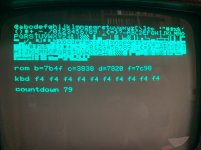
According to the PETTESTER manual, it seems that I have a problem in the ROMs. As BASIC ver. is 2, I guess that ROM B and D are damaged, but which ICs belongs to? UD9 kernal and UD7 BASIC maybe? I have a few 2532 and a 2532-2732 adapter that I can use in my Willem EPROM programmer. Should I try to programm the EPROMS then?

Also, the keyboard codes are not correct but this time I think I guilty. Before to post here, I read that some PET sockets have bad contacts and I set out to change all the sockets beginning by the UC7 one. The result was a disaster and I had to restore the tracks I broke. If I'm not wrong, this IC controls the keyboard so, most probably that's why the codes are not correct.

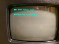
The good news are that the RAM seems to be correct:

2.jpg

Later, I removed the PETTESTER EPROM and installed the original EDIT ROM and I get this screen all the times:

3.JPG

I guess that the problem is the damaged ROMs so, will be the next step to programm the 2532 to replace the ROMs? Are they UD9 kernal and UD7 BASIC ?

Thank you
 
So, it wasn't a bad educated guess regarding UA5 was it?

It is UC7 that is the keyboard PIA. You should not replace anything until we suspect a fault with a component (either by testing or deduction). Even then, if you are not confident in your skills, then buy some 'rubbish' PCBs off eBay and practice your desoldering skills.

Can you post the numbers that are on the ROMs please. That should tell me what ROMs you have, and in which sockets.

BASIC 2 does not have a 'B' ROM (socket UD5 should be empty) so ignore the checksum for that ROM!

The ROM that appears to be 'faulty' is the 'D' ROM in socket UD7 - but this does not appear to be an original ROM, but an EPROM with a bit of black tape on it. Who knows what is programmed into this device?

The display (when you put the EDIT ROM back in) is TIM (the machine code monitor). There are two reasons why TIM could be displayed: 1. Faulty ROM(s) or 2. Faulty UC7 keyboard PIA...

There is a diagnostic pin input into UC7 PA7 (signal DIAG) that forces entry into TIM on a powerup.

It is possible someone has a custom UD7 ('D' ROM) fitted. It may not be faulty, it just may be a custom - hence the checksum difference. Rather than saying 'Commodore' at startup it may say the name of a company or person? Just guessing... You could dump UD7 and we can have a look at it.

Dave
What it seems incredible is that with only a logic probe you found the UA5 defective. Good job Dave!

As requested, the ROM numbers are:
UD9: No reference, it should be in the metallic plate but cannot be read due to the rust.
UD8: MOS MPS 901447 24 1179
UD7: EPROM HN462532G
UD6: MOS MPS 901465 01 2279
UD5: Empty

One important thing to remember is that this PCB was working without problems, but suddenly one day when I turned on the PET I got the garbage screen. The BASIC was version 2 and the RAM 32K, I'm sure about this.

Anyway, if I well understood the next step will be to replace UD7. I will try to reprogramm the chip with my Willem and if it's damaged to programm one of my 2532 with the image in the Zimmers webpage. (basic-2-d000.901465-02.bin I guess...)

Thank you for your continuous support
 
>>> What it seems incredible is that with only a logic probe you found the UA5 defective.

Yes, even I was impressed!

No, I would leave UD7 alone for the time being (unless you have a replacement EPROM you coukd use). Let me checkout the ROM numbers first.

Concentrate on fixing UC7 (using PETTESTER). I can talk you through checking the device with your logic probe.

However, before that, check that each pin of the IC is making good contact with the associated PCB track, and that there are no short circuits between any of the pins. Use your multimeter on resistance with the PET power OFF.

Basically try and sort out any potential socket/solder/PCB track issues first.

If you can, dump UD7 and post it for me to look at.

Dave
 
Last edited:
UD9 is the kernal ROM (F) and gives the correct checksum, so is ok. This should be 901465-03 for BASIC 2.

UD8 is the EDIT ROM (E) and a part number of 901447-24 is correct for BASIC 2.

UD7 (D ROM) should be part number 901465-02 for BASIC 2.

UD6 (C ROM) is part number 901465-01 which is correct for BASIC 2, and it gives the correct checksum, so is ok.

UD5 (B ROM) should be empty for BASIC 2.

Either the EPROM in UD7 is faulty or a custom part. If you have a spare EPROM available (of the correct type) you could program a new part by downloading the binary file for 901465-02 from the zimmers website.

Please do NOT reuse the existing EPROM. It may be OK and a unique version of the firmware?

Dave
 
Back
Top