• Please review our updated Terms and Rules here

Commodore PET CBM 4016 ASSY 8032080 RIFA burn and more

Some people use a 4K EPROM rather than a 2K EPROM (because 4K EPROMs are generally more available than 2K EPROMs).

However, it is usually good practice (in this case) to duplicate the 2K ROM image to make a 4K ROM image.

If you have a 2K EPROM, it is half of the 4K file image...

Dave
 
Well, I guess since a 2716 is what I asked for: I get 16kbit or 2kbyte and the burner will just trunc the second half...
 
Probably.

It may also 'whinge' of course as the EPROM is not large enough to accommodate the file you have asked for. However, most of them would load the first 2K of the buffer (there will be an option for that).

Dave
 
Well so now it is time to wait 2 weeks... Brexit makes the mail go pffffff....
 
Well, I guess since a 2716 is what I asked for: I get 16kbit or 2kbyte and the burner will just trunc the second half...
This is where a Hex editor program is handy, you can just copy the first 2k and paste it into a fresh file or just delete the duplicated second version if that is there. And get the file the correct size for your Eprom and programmer.

There are free downloads, something like this, also useful for file comparison

 
Thanks Hugo, ROM topic is hopefully covered just waiting for the mail.

I'd like to pick your delicious brain and/or your reference library for soldering those old phenolic boards. I have a bunch of those, many equal machines but most with intermitted faults sometimes influenced by mechanical factors (like screwing the board in the case makes it not work or vice versa) but also thermal (machine works on cold start but not after warmup or vice versa). From the very few sources I found, the problem is often cold solder joints, especially on those connecting both sides of the board. i bought a pincentte like measuring head to measure those through connections. however the faults are so fragile that i have a hard time finding them. sometimes i get lucky by manually reflowing the solder joints in an suspicious area. any advise or insights you have in this space?

i have made a post a while ago about one phenolic board i invested a lot of time into and dave was kind enough to help there also ( https://forum.vcfed.org/index.php?t...alculator-division-issue.1245565/post-1348603 ) but i still feel i must know more about these.

thanks, alex
 
Last edited:
Thanks Hugo, ROM topic is hopefully covered just waiting for the mail.

I'd like to pick your delicious brain and/or your reference library for soldering those old phenolic boards. I have a bunch of those, many equal machines but most with intermitted faults sometimes influenced by mechanical factors (like screwing the board in the case makes it not work or vice versa) but also thermal (machine works on cold start but not after warmup or vice versa). From the very few sources I found, the problem is often cold solder joints, especially on those connecting both sides of the board. i bought a pincentte like measuring head to measure those through connections. however the faults are so fragile that i have a hard time finding them. sometimes i get lucky by manually reflowing the solder joints in an suspicious area. any advise or insights you have in this space?

i have made a post a while ago about one phenolic board i invested a lot of time into and dave was kind enough to help there also ( https://forum.vcfed.org/index.php?t...alculator-division-issue.1245565/post-1348603 ) but i still feel i must know more about these.

thanks, alex
You are really asking me to write an essay.

I had a look at that calculator board with the intermittent fault.

On the soldering topic with phenolic boards, the important thing is to never attempt to move a component, or pull on it while heating the solder join. The biggest mistake people make is melting the solder at the same time as pulling or manipulating the part ( this can be ok for fiberglass pcb's, but not phenolic ones) The adhesives which stick the copper foil to the board soften significantly with heat and lift off very easily when hot.

To de-solder a part, add fresh high quality solder to the join (suggest Loctite 64:40 five core solder in the USA or Ersin multicore UK, never use any added liquid fluxes and never Lead free solder). This adds very effective flux.

Then make sure the soldering iron temperature is only about 10 to 30 Deg C over what is required to melt the solder, if its a large area the over-temp value needs to be higher because of the heat extracted from the iron, and use the soldering iron to press solder wick over the pad and component lead wire. This tends to place pressure, if any, on the foils towards the pcb surface.

It pays to use good wick, the best available is Japanese Goot brand made by TAIYO Electric.

You can also use a sucker. Though with good wick for the application it works better, suckers are more helpful with plated through hole modern boards. If the component pin remains stuck to the pad, you can arrange to push the lead wire sideways in the plane of the board surface (not pull up on it). And just a small touch with the iron on the component lead itself, not the whole pcb pad, to free the component lead from the pad. But you don't need to do that most of the time because the wick removes 99% of the solder. If there are components like germanium diodes and germanium transistors, it is best to place a heat extracting pincette on their lead wires, where access allows it.

There are a large number of causes or intermittent faults and many a case the pcb itself is not to blame. The general soldering on your calculator board looks pretty good, though sometimes if wires are oxidized they fail to solder correctly the first time at the factory.

Some intermittent faults can reside inside IC's , resistors, capacitor, diodes and if you are checking for a thermally related fault, the last thing you want to do is spray freeze spray over the general are, because it spreads everywhere and cools down too many parts at the same time. The better move is to use a cotton bud (Q tip in the USA) and dip that into a pcb cleaner, and apply that to individual parts wetting them. For large IC's you can apply a pool of fluid to the top and watch it evaporate while you add more. This cools just the one part as heat is taken away by the latent heat of evaporation of the solvent. It gives a more specific result.

But, the way in which a fault can appear intermittent, does not necessarily mean that there is a defective component failing, or a broken track somewhere. It can simply be that a sector of the circuit is on the borderline of operation. The fault appears thermal in nature because when the parts are heated their electrical properties alter and shift the circuit into a non functional condition. This is where, in fault finding, the best tool you have is the thing between the ears.

Firstly you have to figure out what the designer intended with the circuit and how it is supposed to operate. Then plan tests on it, monitoring parts of the circuit with the scope, to try to figure out when the circuit stops, why it did. Sometimes it is required to set things up with the scope already connected , monitoring critical circuit locations and be ready to observe what has happened when the fault appears.

I had an interesting one with a SOL keyboard a while back where out of the blue, every other day it would stop working for a few minutes and then recover. After monitoring various circuit locations I found that the output from one of the IC's used to scan the keyboard was simply dropping out and disappearing for a few minutes, and it was not a thermal issue.

Sometimes it can require all sorts of trickery to get to the bottom of intermittent problems that reside inside negative feedback loops, the reason being that any change imposed inside the loop is counteracted by the loop behavior. For example in this small TV there was a noisy 100 Ohm resistor inside the H. AFC circuit and it took a while to find, the method used to locate it is explained in that article on pages 13 to 15:

www.worldphaco.com/uploads/RESTORING_THE_SONY_MICRO.pdf


This is only one of the many intermittent faults I have tracked down and the approach may need to be customized.

For example we had a car that intermittently cut out and the engine stopped. It would re-start after cooling down and the fault could go away for some days before returning. Once the engine rotation detector stops, the CPU turns off the fuel pump and the ignition drive for the spark plugs & the fuel injectors. The CPU based ECU stored no error codes and therefore the local auto workshop were totally clueless on what was wrong and why the car cut out intermittently. The problem being; what happened first to stop the engine ? (keeping in mind that for the engine to run it requires, fuel, air, compression, timing and spark the F.A.C.T.S). Therefore I built an "Event Recorder" out of some TTL chips to monitor everything I could, the outputs from the ECU to the fuel pump relay the output of the relay to the pump, the output of the drive to the fuel injectors and ignition coil etc. I discovered that the first event was the output from the fuel pump relay vanished, even though the ECU was instructing it to be ON. Opening up the relay revealed a 360 degree ring fracture around a pin that connected a small relay to the PCB it was mounted on.

When I showed this to the people in the workshop and explained how I found it, they said; "Whats an event recorder ? "

So what I am saying here is that there is no right answer to finding intermittent faults, you have to keep an open mind about what the cause could be and devise a logical test system to suit each case, to be able to track down the real cause. And customized test setups can be required in many cases.

The worst case is when the fault vanishes seemingly for good, as it can be impossible to find it when it is not there. This is why I recommend against ideas like re-flowing solder joints globally on a board. It is much better to disturb as little as possible when the fault occurs and gently track it down with the scope or perhaps cooling applied to individual components. Global soldering, freeze spraying and board flexion can seem sometimes to make a fault go away, but, unless you find the exact fault for sure, it will come back to haunt you.

In any case, everybody who has tracked down and repaired a difficult intermittent fault, like many people on this forum, know how challenging it can be.
 
Last edited:
Thanks Hugo, that was a very good essay. I am sure more readers will find it delightful. Thank you indeed!

On the PETTESTER frontier, I got my two ROMs, one with the PETTESTV04 and one with the adjusted PETTEST4032 from the other posting - both burned on a NEC D2716D

Both do not cause any change in behavior in the machines, unfortunately. No chirp, no image.

To troubleshoot, I have tried to read the ROMs on a XGecu TL866II Plus/Pro reader using the IC AT28C16 DIP24 profile. I read on a another posting that this IC profile should work to read the 2716s. There could be a problem with the machines still, with me reading out the 2716, with the 2716s themselves and the sockets.

In this process, I also popped the original edit ROMs into the XGecu. They get me a PIN error on A0-A7 but I can still read them. I attached the two edit ROM images. I'll try some more things and update here. Thank you.
 

Attachments

  • UserData.zip
    3.6 KB · Views: 0
My PETTESTER does not chirp...

With the PETTESTER installed, what (if anything) do you see on the VDRIVE, HDRIVE and VIDEO signals to the monitor now?

Dave
 
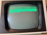
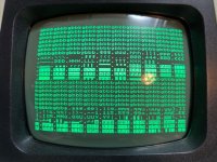
Progress! I am getting convinced the PETTEST4032 ROM was delivered dead to me. I put the PETTESTV04 ROM in, which is the original from you and not supposed to work in my config but I do get screen output now.

In fact I have two machines 4016 and 4032 same mainboard rev with same symptoms. Now both show stuff!!! Nice! At least now we can get the detectives starting:

4016:

IMG_0409.jpeg

4032:

IMG_0411.jpeg
 
Last edited:
Excellent.

So, both of your problems are DRAP-related faults.

The 4032 has a 'hard' fault - it fails the very simple memory test for pages 0 ($0000 to $00FF) and 1 ($0100 to $01FF).

The 4016 has a 'soft' fault - as it passes the very simple memory test but fails when it attempts the full RAM test.

A couple of questions - as you have just shown me a static shot and not a video...

For the 4032 - is the screen content 'fixed' or does some of the screen characters change?

For the 4016 - it should have passed a number of tests before it got to this screen. In particular, it passed the 'simple' page 0 and 1 memory test, but failed when it tried to use it in anger! I am improving my 'simple' memory test for the next issue of PETTESTER (I just have no time at the moment). For this machine, does it contain one bank of 16K DRAM chips or two banks of 8K DRAM chips?

Dave
 
Thanks Dave. Sounds like good news.

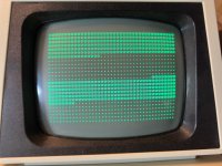
4016: it shows another (or maybe two) screens quickly. The photo above is the final screen. One of the screens before see here:

IMG_0408.jpeg
As for the RAM config there is always alternating RAM and empty. I need to check the numbers later.


4032: i think this screen might also be the second or third screen but once it shows that one - it stays like that. It is also reproducible with power cycles.

The early screens are harder to capture as they need a monitor preheat and then power cycle. They are also kind of dim.


Thanks.
 
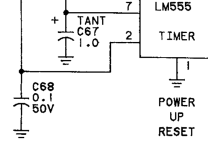
>>> How to reset?

Solder a normally-open pushbutton across C68 (0.1 uF capacitor in the 555 timer reset circuit). Push to reset.

1714136995841.png
>>> Also how to find the bad 4116s I guess?

It may not be a 4116 DRAM of course. There are address multiplexer ICs (E3, E4, E5 and E6) and data bus buffers (E9, E10, I10 and I11) to consider. It is most likely a DRAM fault though.

First thing, are the voltages correct on the DRAM (all of them)? Check +5V, +12V and -5V relative to 0V/GND.

If you have two banks of DRAM, there is a handy little trick to swap over the /CAS signal between the two banks - but I will explain this trick later.

Dave
 
Ah ok, i guess i could short there but installing a button for now seems overkill. will this yield more insight?

has the gggg..... screen helped for your diagnostic?

voltages have been fine on the drams. i have checked about a pair of ics on each machine before. if i need to do all of them i can do it tonight. i do have 1 or 2 spare 4116s also.

i am not sure what a bank is in a pet. i would know in a 486. i guess the 4032 could have two banks? the 4016 i guess not since it only has 8 4116s.
 
It is the same thing in a PET...

If all of the machines have 4116 DRAMs then the 4032 has two banks of 16K and the 4016 has one bank of 16K.

I was just asking, because the 4016 also came in two banks of 8K DRAM chips.

Yes, the g/b has helped me. There is a repeating pattern of one good and three bad (all the same value) but the pattern changes once the address is in page 1 rather than page 0.

This is leading me to think that this particular problem is an address multiplexer containing address line BA8 (possibly).

However, we may be dealing with two concurrent faults.

Let me think after work...

Dave
 
Where would page 0/1 of RAM be located on the board? Closer to the hinge or further? Or is the page spread across the DRAM chips? Also what are the multiplexers? Are these 74xxx ICs?
 
Each 4116 DRAM is one (1) bit wide - so eight (8) of them are required for one full byte (i.e. 8 off 4116 DRAMs are required to form 16KB). So, yes, spread across each DRAM.

There are two (2) rows of eight (8) DRAM chips - each row of 8 chips form a bank.

Bank 0 (one row of 8 chips) covers addresses $0000 to $3FFF.
Bank 1 (one row of 8 chips) covers addresses $4000 to $7FFF (if fitted).

Bank 0 consists of 4116 DRAMs I2 (data bit 7) to I9 (data bit 0).
Bank 1 is J2 through J9.

The address multiplexers are ICs E3, E4, E5 and E6 (74153 TTL devices). They cover RAS-only refresh, RAS address and CAS address. The address lines are multiplexed into the 4116 as two parts (called RAS and CAS) in order to reduce the number of pins on the DRAM chips.

How much experience do you have with your oscilloscope? It is possible to use the oscilloscope (in conjunction with my PETTESTER ROM) to test the address multiplexers out. You can also checkout the data bus buffers (E9, E10, I10 and I11) in a similar manner.

Dave
 
Well we got this far in the journey. See nothing stopping me and my cheap oscilloscope from taking measurements. Which one do we start with? The 4016 with the soft issue or the 4032 with the hard issue. I'd vote for easier one to fix if there is such a machine.
 
Back
Top