• Please review our updated Terms and Rules here

Cromemco dazzler replica project

Looking good so far.

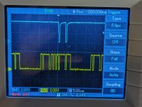
I am guessing the 1 and 2 on the left-hand side indicate the zero reference for channel 1 and channel 2 respectively.

I am also guessing that the blue arrow on the right-hand side is the trigger level. At the moment it is at the bottom. It needs to be halfway between the top and bottom of the indicated signal.

I also notice that the coupling is AC. This needs to be DC for both channels!

See if you can make those changes.

Dave
 
Last edited:
Excellent.

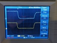
Now you want to speed up the timebase setting to make the low part of the blue trace (channel 1) wider. This will adjust the yellow trace (channel 2) as well.

You need to make the low bit of the very first pulse after the trigger as wide as you can.

Dave
 
If I hold my phone at an angle, I can see that A7 is LOW when the blue trace triggers. This is what I expect it to be.

It will be easier to see if the pulse is wider though.

Dave
 
Spot on!

See, a bit of 'hand holding' and you are now an expert!

OK, so move channel 2 (yellow trace) to A6 now and see whether that is HIGH or LOW.

Repeat for A5 down to A1...

What you should end up with is a series of 0 and 1 for A7..A1.

We know the first logic level, so "0xxxxxx".

Fill in the x's...

Dave
 
Potentially stupid question: should this be before/after I've entered the RDOS commands or does it not matter?
 
cant see the jumpers on board 2 ?

If its the extended pads at IC45, I cant see how they work ? They dont jumpe from anywhere to anywhere ?

View attachment 1275792
Gary,

Just seen your post.

IC45 decodes the address bus A7..A1 depending upon jumpers installed from IC45 back to either the address lines or the inverted address lines.

The PCB was marked J1 to J7 and if you wired jumpers from J1-J1, J2-J2, ... etc. it sets up the default I/O base address of 0Eh.

If you install two (or more) Dazzler cards, each card has to have a unique I/O address (or, more correctly, a pair of I/O addresses), so you have to adjust these jumpers accordingly.

Dave
 
Ok here we go:

A7 IC59P9 = 0
A6 IC59P5 = 0
A5 IC59P11 = 0
A4 IC59P3 = 0
A3 IC59P13 = 1
A2 IC59P1 = 1
A1 IC58P9 = 1
A0 IC58P5 = 0

so, 00001110
 
So that is 0Eh, as it is supposed to be.

So IC45 (and the inverters and 'J' links) appear to be working correctly.

It is too late at night now to think any further...

 Dave
 
Last edited:
Gary,

Just seen your post.

IC45 decodes the address bus A7..A1 depending upon jumpers installed from IC45 back to either the address lines or the inverted address lines.

The PCB was marked J1 to J7 and if you wired jumpers from J1-J1, J2-J2, ... etc. it sets up the default I/O base address of 0Eh.

If you install two (or more) Dazzler cards, each card has to have a unique I/O address (or, more correctly, a pair of I/O addresses), so you have to adjust these jumpers accordingly.

Dave

The distance the jumpers, err, jumped surprised me.
 
OK, next tests...

Set the oscilloscope up as in post #403 again, but perhaps with the timebase just a bit slower to space the two pulses out slightly wider.

With the CPU executing RDOS.

Ch1 (blue) measuring IC45/8 again.

Use channel 2 (yellow) to make the following measurements:

Make sure that IC39 pins 3 and 12 have the same signal present as channel 1.

Check that IC39 pin 2 is HIGH (you might want to slow the timebase down quite a bit to take this measurement and then return it back afterwards).

Check that IC39 pin 1 is the INVERSE of channel 1.

Check that IC48 pin 12 is the same as the above (i.e. the inverse of channel 1).

Check for activity on IC48 pin 13 of any type. Again, slow the timebase down quite a bit.

Check that IC48 pin 11 is LOW. Again, a slow timebase is called for.

See how you get on with these...

Perhaps have a look at the schematic to see what we are measuring?

A bit of 'theory' from yesterday...

The CPU address bus (on a Z80 at any rate) is used to address memory (all 16 bits from A0 to A15) and I/O ports (the lower 8 bits from A0 to A7).

How does the Z80 differentiate whether the address bus is being used for memory or I/O accesses? The answer is the control signals /RD, /WR, /MREQ and /IORQ.

The S-100 has its own control signals used to specifically identify I/O reads and writes (SINP and SOUT). The CPU card forms these control signals from the Z80 signals via a bit of logic.

Now, the CPU is running RDOS out of ROM between addresses C000h and C3FFh (for a 1K RDOS ROM at any rate) and is, therefore accessing memory using the address bus.

The Dazzler logic (via IC45) is decoding for I/O port adress 0Eh and 0Fh using the lower 7 bits of the address bus (A1 to A7). However, at the IC45 level, it is not known whether a memory address or an I/O address is being specified by the CPU on the address bus. This is only determined by the logic later on by gating SINP and SOUT.

As a result, IC45 will decode not only I/O ports 0Eh and 0Fh, but memory addresses C00Eh, C00Fh. Not only these, but more addresses such as C10Eh and C10Fh. In fact any memory address XX0Eh or XX0Fh.

Therefore, as the CPU executes the RDOS firmware it will (occasionally) execute the odd instruction (or read from or write to memory) at address XX0Eh or XX0Fh. It is these memory addresses that we are looking for to check that the 0Eh and 0Fh decoder (IC45, the inverters and the jumper wires) are all correct.

The tests today are moving on to combine the IC45 decoding (that we now know works from your testing yesterday) with the logic further down the line...

I hope this makes sense?

Dave
 
Last edited:
Just thinking aloud here...

When you performed the tests (with the logic probe?) back in post #382, your logic probe does have a 'pulse catcher' feature doesn't it?

If not, there is no possibility of the human eye 'seeing' this pulse otherwise...

 Dave
 
Thanks so much for explaining the theory. I actually never knew the ports are just the lower 8 bits on the address line, I was always confused about how ports were really "addressed" - so these lines are shared.. and cards react to these addresses, depending on control signals.. This all makes a bit more sense now.

Make sure that IC39 pins 3 and 12 have the same signal present as channel 1.
Yes, exact same signals.

Check that IC39 pin 2 is HIGH (you might want to slow the timebase down quite a bit to take this measurement and then return it back afterwards).
Yes, Pin 2 is HIGH

Check that IC39 pin 1 is the INVERSE of channel 1.
Pin1 is doing nothing, it is LOW.

Check that IC48 pin 12 is the same as the above (i.e. the inverse of channel 1).
This pin is also doing nothing, LOW

Check for activity on IC48 pin 13 of any type. Again, slow the timebase down quite a bit.
No activity on IC48P13

Check that IC48 pin 11 is LOW. Again, a slow timebase is called for.
IC48P11 is LOW.

When you performed the tests (with the logic probe?) back in post #382, your logic probe does have a 'pulse catcher' feature doesn't it?
I'm sorry but I don't know what you mean about a pulse catcher?
 
Last edited:
Back
Top