• Please review our updated Terms and Rules here

Data Extraction project MC1468705G2.

Hugo Holden

Veteran Member
Joined
Dec 23, 2015
Messages
4,805
Location
Australia
I thought I would start a new thread on this and a summary of what transpires.

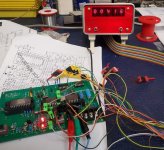
This has been built to help solve a problem that has been bothering me since the 1980's, how to replicate this IC for one of my vintage Conrac VDU's. The original ROM file is not available. I want to extract the file from the original IC in the VDU.

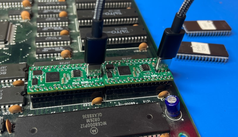
I have just finished the Programming pcb for this CPU-Eprom IC. I thought I would do a professional job on this project, no breadboard wires to cause troubles and foul up the experiments. I followed Motorola's pcb design fairly closely but added some headers to connect to the data lines and some jumpers to disable the clock and use an external slow clock. And disable the programming voltage too. It took me a while to acquire all of the parts. It works by loading a program from a ROM like a 2532, into the CPU's-ROM and then verifying the file. This firmware is in the CPU.

The idea, initially at least, is to get used to programming some of these blanked CPU IC's with a known array of bytes.

Once that is accomplished (which is not the hard part I suspect) then comes the tricky part:

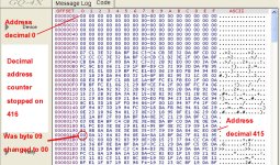
It was suggested by Daver2 that the CPU probably contains an undocumented protocol (firmware program) where it will output the internal ROM byte file. It is a matter of trying to tell it to do it, by manipulating some pin voltages. I will know if I have succeeded because I will know the byte array in the trial IC.

I don't know yet if this will work, but I am hoping it will. I will report the findings on this thread later.
 

Attachments

  • AN907A.jpg
    AN907A.jpg
    724.1 KB · Views: 33

Attachments

  • Microcontroller EPROM Programming (Computercraft, Aug 92).pdf
    460.6 KB · Views: 2
Clean layout. No luck finding an accessible copy of that AN907A online; can you share a pointer?

(Yumpu appears to have one locked away as "ePaper" :-<.)

I did however find an interesting article entitled "Microcontroller EPROM Programming" starting on page 23 in:

I can see it on this website, a little jumpy with advertising banners, but all the pages are visible, it might be something to do with your browser. I am working with a paper copy, worse case I could scan it.


It is interesting how some things in life, over the years that were once on the net or elsewhere, can disappear, like Will Robinson's bottle of Carbontetrachloride.
 

Attachments

  • CCL4.jpg
    CCL4.jpg
    53.6 KB · Views: 10
Thank you, but as I said, yuk with Yumpu. After a little better/more thought I found the attached original PDF and OCR'd it for good measure :->.
 

Attachments

  • AN907A_REV0_Programming_The_MC1468705G2_Microcomputer_EPROM.pdf
    486.8 KB · Views: 11
Don't know if this is helpful, but this may document the process to read the EPROM contents if the original developer enabled that.

https://ia600304.us.archive.org/0/i...5EVM_Evaluation_Module_Users_Manual_Dec83.pdf

I think this is relevant to the part you are discussing. Specifically page 3-19. Hopefully whoever made the code for your part was lazy and did a reference implementation. The code and readout interface is described around page 3-28. Another common trick was to implement the code, but require a "secret code" of I/O lines or use alternative I/O lines.

-- Bob
Thanks, That evaluation module is quite something.

So it appears that the thing is that the dump program is not something Motorola supplied the Chip with, but it is put in there as an option by the end user. Possibly given the paranoia about firmware security, some manufacturers may not have done that and put the code in. But it was the early 1980's.

Any suggestions about how to modify/set up my programmer board based on this new information, to attempt the dump, would be helpful. I might have to make up a serial interface so it can send the dump to a terminal. If it has a secret code required, that could be bad. I would have to build a device that tried every possible combination.
 
So it appears that the thing is that the dump program is not something Motorola supplied the Chip with, but it is put in there as an option by the end user. Possibly given the paranoia about firmware security, some manufacturers may not have done that and put the code in. But it was the early 1980's.
I am guessing they didn't, not because they were worried about security but simply because that code takes up extra space in the EPROM that they'd likely want to use for their own code. (There's not exactly a massive amount of EPROM in these things.)

Any suggestions about how to modify/set up my programmer board based on this new information, to attempt the dump, would be helpful. I might have to make up a serial interface so it can send the dump to a terminal. If it has a secret code required, that could be bad. I would have to build a device that tried every possible combination.

From reading the previous thread (and the one before that) I my guess is that the "run built-in program routine without Vpp and then see what the verify says" approach may be the one most likely to work. ROM emulators are not too hard to build: as mentioned in the other thread, you can use a static RAM with some tri-state buffers such as 74x245 to switch between the ROM interface on the target and a separate RAM interface that the host can use to load the ROM. But it's much easier these days with super-fast microcontrollers (so long as someone else has already written the software): check out the PicoROM.

in_use.jpg
 
I've been going over this chestnut again, and I cannot see how the verify function is of any help:

After the bootstrap loader built into the CPU is initiated , it transfers the entire file from the external Uveprom, into the internal one. After completing that process, it then goes on to run the cycle of addresses again to verify the internal programmed ROM contents match the external ROM, but the thing is, it lights the verify light at the end, only if both files match (which means it has assessed the entire file), but if they don't match, it simply sits there like the Tar Baby, doing nothing, doesn't light the verify light at all.

The whole thing looks like a one way trip of data into this MCU, and probably was the best data security ever invented.

If it had a system where it lit a "non-verify" light as soon as a byte mismatch was encountered, there may have been some hope using that signal combined with a ROM emulator and trialing for matching bytes.
 
Ah, I see what you're getting at there. Yes, that is a bit of a conundrum. I wonder if there's any external information available about the bootstrap loader code. Is the source or object code for that programming tool available? That could provide some clues. Otherwise, I suppose it means looking at the pins to see if it's changing any external state beyond the "verify" output.

If you want to get really into it, it's possible that analogue state is changing as the program runs even if the digital state is not, so you could use the standard cryptographic techniques of looking at the voltage levels on various pins, power usage, and so on to get clues to the internal state.

It had also occurred to me that stopping the clock might be useful.
When I built the programmer board, I made provisions with links to disconnect the 1MHz crystal clock, so and to inject a very slow clock of around 1Hz. The manufacturers say the chip is fully static and works down to DC, so that is helpful.

The problem really is that all of the signals that are unique to the programmed bytes in the MCU's ROM, remain inside the MCU. I think the input data gates & buffer currents would not induce enough reliable voltage change to indicate conditions inside the chip, whether the byte in the internal ROM, matched the ones being compared with the outside ROM, the bytes of which are probably placed in a register in there too before the comparison. I cannot see how the byte data match or mis-match could be easily detected externally by subtle voltage changes on any pins, but I guess it might be possible for the CIA . Power supply voltage transients alone would dwarf everything else, it would have to be powered by batteries in an electrically quiet environment, but even then..

I don't know if the bootloader code is available. @daver2 was wondering if this MCU may have contained undocumented code to export the ROM file, but we may never know.
 
Last edited:
I cannot see how the byte data match or mis-match could be easily detected externally by subtle voltage changes on any pins, but I guess it might be possible for the CIA .
I was thinking perhaps the MCU had a mode that could bring out external data and address buses, like the 6801, but apparently not. So the bootstrap code must be using the PIAs to generate addresses and read data from the external ROM. Though then it does occur to me, most likely the the verify routine is (re-)reading the data from the external ROM byte by byte to do the compare for the verify, so you should be able to see how far it gets by monitoring the addresses you see sent to the external ROM, right?

As a side note, I keep on forgetting where my copy of the datasheet for this IC is; for future reference (my own as well as others'), it's here.
guess that is possible, but it looks unlikely to me that it stops at the address when an error is found in the byte match, I got the impression from the data sheet, it checked the whole file and then decides to light the verify light only if there is a match.

But, I will look at the address values with some experiments to see what address it stops at. I can create a file for the MCU and an altered file for the external ROM, and I could corrupt the external rom and see it there is a stop in the addressing, or not.
 
guess that is possible, but it looks unlikely to me that it stops at the address when an error is found in the byte match, I got the impression from the data sheet, it checked the whole file and then decides to light the verify light only if there is a match.
Well, it has to check the whole range before it can light the verify lamp, of course. But from a programming point of view, it's easier to stop completely as soon as the first byte mismatch is found, rather than store that information and carry on looking for more matches or mismatches. (Probably more importantly, given that the whole thing with the programming algorithm has to fit in 240 bytes, it also uses less code to stop immediately.) So I think there's a good chance it will stop at the offending address, thus letting you use a ROM emulator to try out byte 0 values until you see the address increment to 1 before a stop, then try again with byte 1 values, etc.
 
Well, it has to check the whole range before it can light the verify lamp, of course. But from a programming point of view, it's easier to stop completely as soon as the first byte mismatch is found, rather than store that information and carry on looking for more matches or mismatches. (Probably more importantly, given that the whole thing with the programming algorithm has to fit in 240 bytes, it also uses less code to stop immediately.) So I think there's a good chance it will stop at the offending address, thus letting you use a ROM emulator to try out byte 0 values until you see the address increment to 1 before a stop, then try again with byte 1 values, etc.
I will set up the experiment, I have a type of multi-channel logic probe to monitor address values and display them, and I can do the test in slow motion by slowing down the clock rate.
 
  • Like
Reactions: cjs
Oh, it also occurs to me that if you have trouble figuring out the output, the bootstrap code is available in the system memory map, and so it's not too hard to write code for one of your unprogrammed devices that would dump that code via one of the PIA ports. I've not done 6805 code, but I've done plenty of 6800, so I'm happy to give this a go and disassemble/reverse-engineer the result, if that's helpful to you.
 
Oh, it also occurs to me that if you have trouble figuring out the output, the bootstrap code is available in the system memory map, and so it's not too hard to write code for one of your unprogrammed devices that would dump that code via one of the PIA ports. I've not done 6805 code, but I've done plenty of 6800, so I'm happy to give this a go and disassemble/reverse-engineer the result, if that's helpful to you.
That is an interesting idea, because there might be something hiding in that boostrap code that could help. Also there are 5712 bytes and 5 bytes before and after the boostrap, that says are "unused" I wonder if that is true, or if there could be some code hiding there so we could dump that too, just in case.
 
Last edited:
  • Like
Reactions: cjs
.........it might take me a while to complete the tests, I'm waiting for a 68766 UVeprom to arrive in the post. I was using a 2532 but it is not suited to the mask set version of the CPU I have, I need the 8K ROM.
 
@cjs you were right !

I set the system up with a 4k 2532 ROM, but strictly I should be using the 8k one for the MCU's I have, but it didn't matter for the experiment. All that happened is the file essentially just repeats itself for the upper 4k not having an A12 address line.

Some years ago I had made a binary to decimal logic probe that shows the decimal equivalent of the binary value, it only has a latency of 350nS, I used this to monitor the address lines A0 to A12. I programmed a blank MCU with a trial file in the 2532 ROM, it programmed and verified ok.

I noticed watching the the probe display that the address counter counted up to something like 2xxx decimal, changing a little fast to see (the system is running the on board 1MHz CPU clock), that the verify light came on and the address lines went to zero.

There is a select switch setup on the programmer board to program and verify, or just verify. There are two other switches that remain enigmatic, I'm still investigating those.

I then put the 2532 ROM back in the GQ-4x programmer and altered one byte at address 1A0 hex, from 09 to 00. And then ran the verify again, the address stopped on the exact address of the defective byte ! and of course because it never got to the end, the verify light did not come on.

I now need to devise a contraption to step through all possible bytes at each address with a ROM simulator, and an output to control the verify circuit and keep a record of each successful byte trial. I think I can do it with my SOL-20 and I can do some 8080 assembly language programming and use the parallel port, or maybe my IBM5155 in 8088 assembly, I have played around in the past manipulating the ports. I have no experience doing such things via USB ports on modern computers.

The other possibility, that could suit me, is to do the whole thing in hardware (which is what I mainly do) and transfer the successful byte match into another ROM at the correct address directly, or a non-volatile RAM would be easier, I have plenty of spare FRAM from other projects,, so as to re-create the original file, likely it would only take some hours or overnight. Any suggestions welcome.

I think if I detect both the rising and falling edges of address line A0 (to effectively create a frequency doubled signal to use as a clock for a hardware circuit to transfer a latched trial byte to non volatile SRAM) it will work because this address line only changes state (to the next address) if the previous byte matched.

Thank you for the help so far.

I am now convinced for the first time, in about 40 years, it is possible to extract the file from this MCU and make a duplicate. I'm glad I built the programmer board, it was a pretty expensive exercise.
 

Attachments

  • ROMtest2.jpg
    ROMtest2.jpg
    244.4 KB · Views: 3
  • Romtest.jpg
    Romtest.jpg
    562.6 KB · Views: 3
Last edited:
Back
Top