• Please review our updated Terms and Rules here

Replicating a programmed MC1468705G2 Computer-EPROM

Hugo Holden

Veteran Member
Joined
Dec 23, 2015
Messages
4,645
Location
Australia
I have a very special VDU that uses this IC in its control system and looked at this problem before, but never convinced myself there is a way to do it, yet.

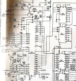
I want to replicate the IC. It was programmed at the factory. I can get blank IC's

The information to build the programmer for it is in this document, I can easily build this hardware and or modify it (if I have a sensible plan), but the problem is more complicated, to extract the original Eprom file:


I could wire it up without the Vpp voltage connected, to prevent damage to the original file/IC.

The boot loader inside this IC is designed to program the IC from a file held in an external eprom (such as an MCM2532) on the programming pcb. Clearly this internal firmware sequentially address a byte in the external eprom, programs it into the internal eprom, one by one. When that loop is finished, the internal firmware then runs a second verify loop, to compare its own internal eprom programmed bytes, one at a time with the external eprom, if they all match it throws up a verify light at the end of that loop.

The trouble is the firmware program in there has to complete a full loop of all the bytes to be checked and I don't know, if in verify mode, if that loop terminates at the moment it sees the first mismatched byte, if that was the case it might help the problem, because a rom simulator could be put in the external eprom socket and the address value remembered by an external device, to find the location where it didn't match, then the byte there could be tweaked until it matched and then incremented to the next address. Does that sound plausible ? But since the verify light only comes on if the whole file is good, that signal cannot be used to capture an address. Or the address where it stopped, might remain there on the address lines to the external eprom, I don't know.

(imagine that an IC that programs itself, it is like Daleks building themselves in factories)

The thing that I'm wondering: At any time in this program or verify process, would the data corresponding to the byte values in the internal Eprom, ever appear externally on the IC's pins, so if the process was slowed right down, with a very slow clock, the data values could be read ? But I think they probably remain internal to the IC and are "locked in", like the ultimate form of file security.

Or, is there any way anyone can think of, that the IC's external connections or function can be manipulated to view its internal eprom data or any system or method that might work ?

(There are some bytes that need to be programmed for the clock system etc, but probably I could get those right by trial and error).
 
Last edited:
Well, as far as I can tell, they're all the same basic family; I'd say it was worth a try.

There's also this

Apparently, the HC devices are a different story.
The thing is I'm not clear on what to "try" for my IC.

That link looks a little more promising using NOP's than trying to do it looking for small timing differences as Peter did, but still, I would need some fairly detailed instructions on how to actually get a hardware setup to work to retrieve the byte file.
 
From looking at the NXP documentation it looks like as though the NOP instruction is not the whole truth...

There appears to be this special "test mode" that is entered by suitable manipulation of the voltages on the /RESET and /INT pins. One of the functions of this "test mode" is the bootstrap mode that performs a self programming and verification activity.

However, buried in the NXP documentation, it states that when "test mode" is entered the CPU reads a port value and uses that to determine which internal ROM program to execute. The implication being that the "bootstrap" program is the default. If this is true, I suspect that wiring the resistors to the port in a NOP pattern causes one of the special internal ROM programs to be executed that has the desired effect of 'dumping' the internal ROM to the outside world.

If you think about it, there were commercial programmers for this device - and these included a VERIFY option that didn't take a week to run! Therefore, there must have been some "undocumented" feature that was never released to the general public - and this is what the commercial programmer units used. Unless the programmer was just using the fact that the VERIFIED digital output went active to signify a correctly programmed part. However, this (in my opinion) is not how a professional device would operate. I would expect to be able to obtain a checksum (or similar) from the programmed device. This would have involved reading back the contents of the programmed device itself.

See https://www.nxp.com/docs/en/application-note/AN499.pdf section 3.1 third paragraph.

This statement is also interesting:
1674226476255.png
There appears to be quite a lot of internal ROM dedicated to the "additional demonstration routines"... Perhaps this masked ROM size is related to the later devices though?

I will have another look around and see what I can find...

Dave
 
Last edited:
I believe that the bootstrap programming code gets copied to RAM, run for programming, then modified to run the verify process. At least that's what I've read.
 
That would be great, if the IC contains the program already in it to dump the contents to the outside world. Thanks Chuck(G) & Daver2 for helping figure out a way to do it if you can. I'm ready with the soldering iron.

Presumably if it did, I would need an arrangement to capture the bytes from the port. I could always wire up a UART IC and send it on a serial link to my computer. Just have to figure out how to send it a byte at a time, depending on how fast they appeared on the port. But I'm patient enough to step through it a byte at a time, if I had to.
 
Last edited:
I did read that you can configure the oscillator in different modes (crystal, RC, external etc.). The device specifications imply that the device clock can be completely stopped and, therefore, single stepped.

Dave
 
been there, done that
have the logic analyzer traces to prove it
it is possible to use Non User Mode to dump the code and the bootstrap
there are a bunch of examples around associated with 705 devices in MAME
what you end up with are logic analyzer dumps of data coming out of the parallel I/O pins
that repeat as the address counter wraps, so one of the things you have to do is figure out
what is address zero and synchronize the data.
it isn't as simple as a serial bitstream coming out of a pin

the whole process is very annoying because of the differences between the nmos and cmos
parts, and the fact there are dozens and dozens of variations of that little part
 
, so one of the things you have to do is figure out
what is address zero and synchronize the data.
it isn't as simple as a serial bitstream coming out of a pin
Maybe though, in a slow single step mode, the first byte of data that appeared on the port would be the first location of the internal UVeprom ? Unless they read it out backward from end to beginning, but that would seem less likely, though maybe it is easier to decrement a counter to 0 and detect that in the zero flag, than increment it to some number and detect that with a comparison and then check the flag, either is possible I guess.......
 
............one thing I can do in the meantime, is that I can build the programmer board. Then I could start with using a blank/unused CPU-eprom IC (which apparently has all bytes 00). I could then put in a 2532 in the external ROM socket in the programmer board. And have it programmed for all zero byte values too. Then I could experiment with the programming voltage deactivated, to see if I could get it to verify that the contents of the CPU- Eprom (which should be bytes 00) matched with the external ROM. At least if I got that working, I could be confident I could transfer the real CPU-Eprom from my VDU later, into that board setup, do at least a dummy program run and verify, without the risk of damaging it or accidentally re-programming my one and only programmed CPU-Eprom IC.

If it turned out that the programming voltage had to be actually present on the CPU-eprom pin, to initiate the programming then verify sequence, that would be somewhat of a risk and it would pay not to let my original CPU-eprom IC anywhere near the programming board and not attempt any tests on it in any board that had programming voltages present.

But also I could program a 2532 with some unique bytes at the beginning of the address range, and some different unique bytes at the end of the file range, and program that into the blank CPU-Eprom on the programmer board. Then if we figured out to read bytes out of the CPU-eprom content out to the port, albeit slow stepping, we could know what the address (because we know where that byte was in the 2532) was and what order the bytes were coming out, in case they come out in a backward sequence.
 
Last edited:
My thought is that you have to apply a high voltage to one of the device pins to get it to enter test mode, but you don't need the higher programming voltage itself.

I also now see that the original work (with the NOP readout method) was undertaken with the smaller 28 pin package and you have the 40 pin package. Is my assumption that your device is the 40 pin package correct?

I see from the various device datasheets that the means of entering test mode seems to have changed between variants of the device. This was confusing me yesterday - but now I understand...

If you have a 'blank' device that could be used to experiment with first, that would be the ideal solution of course to save damaging the original!

I will see if I can work out how to translate from the 28 to 40 pin device later on today.

Dave


Yes, the 40 pin package.

These are the ones I have bought, a few of, to experiment with, they match the IC in my VDU:


I am having my pcb maker prepare the Motorola programming pcb from the AN907A document.

Thank you so much for helping, Dave.

Hugo.
 
Hugo, can you point me at the AN907A document please?

After reading loads of datasheets on this range of microcontrollers I have come to the conclusion that the entire range is one confusing mess when it comes to programming, verifying and these 'special' internal modes of operation!

Never mind, let's concentrate on the matter in hand...

Because of the differences across the microcontroller range, you definitely need to keep your precious microcontroller safe and we can experiment with a 'sacrificial lamb'!

Some of the older 6805 devices appeared to have a NUM pin (non user mode) that was supposed to be tied to GND for normal operation. However, some enterprising person found that by connecting this NUM pin to +5V caused the microcontroller to 'dump out' the internal memory contents. They did this by 'forcing' the PA port to a NOP instruction ($9D) via 1k resistors. This caused the address information to be output on the PB port and selected bits of the PC port, followed by the internal data byte (ROM, BOOTSTRAP ROM, RAM, registers and I/O ports) on the PB port. It would appear (from the write-up) that the reset vector was read - but overridden to $9D9D by the introduction of this special mode. This caused the internal address register (Program Counter?) to be initialised to the 11-bits of $9D9D as the starting address to dump the internal memory from. It appears that the microcontroller just sits in this mode until you reset the device.

Port B was wired to a logic analyser (along with the external 1 MHz clock signal) in order to capture and analyse the address and data stream.

It would appear that later microcontrollers in the family disposed of the NUM pin - but made PC0 into a multi-purpose pin by applying a strange voltage to it. This was described in the schematic of a 68705 P3/P5 dumper I have seen. +7.5Volts is applied to PC0 via a 1k resistor and this causes the microcontroller to enter this special mode.

I am just now postulating whether the MC1458705G2S works in a similar manner. With it being a 40 pin device (instead of a 28 pin device) I am guessing that PORT A and PORT B would be the same. PORT A wired (via 1k resistors) to form a NOP instruction ($9D) with PORT B driving the internal data bus to the outside world.

We now have to work out how to wire pin 1 (/RESET), pin 2 (/IRQ), pin 3 (VPP), pin 28 (PC0) and pin 37 (TIMER).

These would be my initial guesses (based upon pin translations from the 68705 P3/P5 dumper schematic I have found):

Pin 1 (/RESET) had a 1k resistor to +5V and a link (switch) to 0V.

Pin 2 (/IRQ) - Need to think long and hard about this pin... The /IRQ pin also appears to have a negative voltage on it when programming?

Pin 3 (VPP) was wired to +5V. May need to double check this... I see the programming voltages are NEGATIVE for this device and not POSITIVE. I think for an MC1468705 that this pin may need connecting to 0V?

Pin 28 (PC0) - Need to think long and hard about this pin...

Pin 37 (TIMER) has a 1k resistor to +5V.

For an external clock: pin 38 (OSC2) should be not connected and pin 39 (OSC1) should be connected to a TTL clock (1 MHz?). I am assuming that this pin could be connected to a much slower clock signal to slow things down a bit. The device appears to be of the static design. I remember reading that somewhere.

The data sheet indicates that the TIMER, /IRQ and /RESET pins are significant. However, only programming mode is detailed. Still not sure about the PC0 pin. I am concerned that if we apply too high a voltage to the wrong pin that the 'sacrificial lamb' will be sacrificed!

That's what I have gleaned from this morning's reading at any rate.

Dave
 
Last edited:
Hugo, can you point me at the AN907A document please?


Dave
The link to the document is in post #1 of this thread. It has a sensible pcb layout for the programmer. It is interesting those negative programming voltages (figure 6 on the document) and the /IRQ being held at max -12V (by the zener) for programming,and it looks like a voltage reference of -14V from the emitter of Q4, via Q2 is sent to the programming pin when PD7 goes low. It looks like when Q1 is off (not programming) and Q2 is off too, Q3 clamps the programming pin to gnd. So perhaps then at all other times the Vpp pin should be 0v, but I think I read somewhere it was tied to +5v in use, I'll check the schematic in the VDU.
 
Last edited:
Thanks for the link. That'll teach me to read first...

I have read so many documents today - and they all look similar...

I suspect the negative voltages are to do with the CMOS process of the MC14685G2S as opposed to the positive voltages of the other devices?

The voltages for /IRQ and TIMER are consistent with what I have seen in the documentation for programming.

There must, however, be some other 'twist' to get into this non-user mode as opposed to programming mode. This is going to be the challenge...

Dave
 
In the actual VDU, circuit fragment attached, it runs with the Vpp pin 3 grounded, as it does in the programmer board when it is not programming itself.

Also in this circuit the CPU is clocked by an independent oscillator into pin 39 and pin 38 is n/c,( unlike the arrangement on the programmer board). So this would be the configuration to clock it pulse by pulse from a slow speed source into pin 39.

If it did work( a self byte dump), we might be able, by trial & error, to figure how many CPU clock cycles made the next byte appear on the port. Then I could design a circuit to apply the correct number of pulses after a button push. Since I don't have a logic analyzer, I could just connect a couple of Hex displays up to the port (like two TIL311's) to display the byte and then just document all of them manually, or maybe the UART idea to send them to my computer.
 

Attachments

  • EPROMCPU.jpg
    EPROMCPU.jpg
    309.2 KB · Views: 7
Last edited:
Back
Top