• Please review our updated Terms and Rules here

Diagnose issues: PET 4032 with PETTEST ROM

I use a DIL connector that clips over an IC. The clip can take wire attachments that have a clip at the other end - so you can attach the probe ground clip onto the same IC as you are probing. You can also use the same trick for the probe itself so you have hands-free operation.

Dave
 
I use a DIL connector that clips over an IC. The clip can take wire attachments that have a clip at the other end - so you can attach the probe ground clip onto the same IC as you are probing. You can also use the same trick for the probe itself so you have hands-free operation.

Dave

I like the DIL clips.

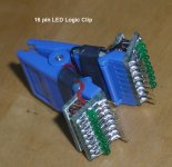
Back in the 1970's there was a version that had LED's in it to show which pin was high. It acquired its power from whatever pin was powered (which is not always pin 14 or 16). The powered pin had the brightest LED. Other pins varied in brightness depending on the pulse duty cycle.

Then these LED logic clips all but disappeared from popular electronics culture, probably the last company to supply them was RS in the UK. They may still have them, or they may not be available. But as I recall they got really expensive.

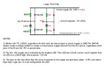
I found some plain blue DIL logic clips, so I added my own LED array to them with some proto pcb material , diodes & resistors.

The advantage is that all the IC pins are still there, for easy connecting to the scope, or to get an earth too. I had no idea what was in the original LED probes, so I designed my one from scratch (circuit attached) but I would think it must be similar to the commercial ones.
 

Attachments

  • LOGICPRB2.jpg
    LOGICPRB2.jpg
    136.9 KB · Views: 11
  • logicprobe.jpg
    logicprobe.jpg
    187 KB · Views: 11
Will something like this work? Is the spacing between pins the same for all 16-PIN DIP packages?

These are the common ones made by 3M

 
I just had a 2001-16N with defective video ram. The piggy back method allowed me to pinpoint which chip was bad but observing the change, but it did not "fix" it. It improved the output but it was still not correctly displaying.
 
I did find a couple of strange things.

Right at the beginning of the first video, the 'default' trace base is at the bottom of the screen (where, in my opinion, it should be for using a single beam - maximise the screen height to view the waveform being measured). However, shortly after that, the baseline then appears in the middle of the screen? Did you adjust any settings in between? If not, where does this standing DC level come from I ask myself.

I observe a couple of signals that appear to be permanently low or permanently high. However, without adjusting the timebase (making it slower) I can't say that with any degree of certainty.

Unfortunately, random poking with a scope probe, generally raises more questions than it answers - unless you are really lucky.

Perhaps you need to soend a little time investigating my two observations above?

Dave
 
I was just reviewing the thread posts. Did your replacement 4116 devices turn up?

I was suspecting UA19 (D0) as being faulty wasn't I?

The other question I am going to ask is - have you made a NOP generator up? This is a couple of 40 pin IC sockets and a few resistors. Alternatively, you can purchase a spare 6502 CPU and 'butcher' the data lines to permanently tie them high or low in the pattern $EA = 1110 1010.

Dave
 
Last edited:
..

Right at the beginning of the first video, the 'default' trace base is at the bottom of the screen (where, in my opinion, it should be for using a single beam - maximise the screen height to view the waveform being measured). However, shortly after that, the baseline then appears in the middle of the screen? Did you adjust any settings in between? If not, where does this standing DC level come from I ask myself.

..

Dave

I noticed that as well and was wondering what had happened. Then it occurred to me that pin 1 is -5v rail, and I'm guessing the probe must have been attached right at the very beginning, making it look like the base was at the bottom of the screen.

Another thing I noticed was that pin 2 looked different to pin 14. These two pins should be tied together, so I'm guessing the machine crashed while using the osilloscope.
 
Ah, that accounts for the 'base level' issue.

Yes, pins 2 and 14 are data in and data out and should be connected together.

The problem is, with an oscilloscope, you really need a plan of how to go about the diagnosis of a problem. Using an oscilloscope on its own, without trying to reduce the 'problem space' is like looking for the proverbial needle in a haystack.

Hence the NOP generator. The CPU should constantly READ from every location, and we should be able to see the address lines on the RAM address multiplexers along with the refresh address lines and then, with a bit of playing with triggers, the multiplexed address lines on the RAM chips themselves. In this case, the data lines will just have garbage on them (whatever default values were in the RAM on power-up).

In the meantime, I would look for data lines that do not have any activity on them (even when you adjust the timebase). Look for permanently high or low signals.

However, because of the data in / data out issue you should really be monitoring the data line only when a RAM READ is active. At any other time you will be monitoring other activity and not what you are looking for...

Hence the reason we need a plan...

Incidentally, for the above reason, I don't think you will find any 'stuck' data lines - otherwise my PETTESTER would not work!

Dave
 
Hence the NOP generator. The CPU should constantly READ from every location, and we should be able to see the address lines on the RAM address multiplexers along with the refresh address lines and then, with a bit of playing with triggers, the multiplexed address lines on the RAM chips themselves. In this case, the data lines will just have garbage on them (whatever default values were in the RAM on power-up).

I have a ROMulator, and https://github.com/bitfixer/bf-romulator indicates that dip switch index 12 is a NOP generator. Can I use this?
 
Of course you can, that's what it is designed for as well...

You will also see that my PETTESTER is in there also at index 13...

Dave
 
Thanks for bearing with me! Unfortunately I'm a software guy and not a hardware guy (but learning more each day).

When I have the ROMulator set to NOP generator, where should I place the probes on UA 19?
 
First off I would check the following pins in the order I have specified:

UE8 pins 2, 4, 6, 8, 17, 15 and 13. These pins should have square waves on them with each successive pin being half the frequency of the prior pin.

Next would be the two ICs in the order specified:

UE9 pins 2, 4, 6, 8, 17, 15 and 13.

Followed by:

UE10 pins 4, 6, 8, 17, 15, 13 and 2.

Note that UE10 has the same pin numbers as UE9 - just in a different order.

Again, these pins should have square waves on them with each successive pin being half the frequency of the prior pin.

UE8 multiplexes the row refresh signal onto the address lines of the RAM.

UE9 and UE10 each multiplexes half of the buffered address lines onto the address lines of the RAM.

Let's just see if everything is as it should be before we look at UA19.

Dave
 
Quick check in to make sure I'm doing this correctly:

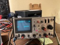
Pin 2 on UE8:
8 divisions. Sec/div = 2 microseconds = 0.002 ms
8.2 * .002 = 0.0164
61 Hz = pin 2

pin2.jpg


******

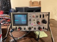
Pin 4 on UE8:
6.5 divisions. Sec/div = 5 microseconds = 0.005 ms
6.5 * .005 = .0325
30.77 Hz = pin 4 on UE8

pin4.jpg
 
I would have to check the schematics again for the exact frequency (as a double check) but your method looks good to me.

Dave
 
The frequencies seem much too low to me.

1MHz should be going into UD3 pin 13 and divided down by 2 to give signal RA1 (0.5 MHz). This should give a 2 us period - but that seems too fast to me for DRAM refresh...

Your 61 Hz is 16 ms which is too slow for DRAM refresh.

My brain hurts :).

There is something wrong somewhere, I just can't work out where for the moment...

EDIT: Ah, worked it out. The DRAM should be RAS refreshed every 2 ms (or faster) for ALL of the 128 RAM rows. This equates to 2/128 ms = 16 us/row (or faster). It is, therefore, more likely that my 0.5 MHz (500 kHz) for RA1 is correct (IMHO).

Can we now work out where the discrepancy with your measurement has occurred?

Dave
 
Last edited:
Ok, just to make sure I'm not doing anything dumb. Here are the pins I used:

chip.jpeg


The oscilloscope is on 10x magnification for horizontal. Does this affect anything?

Is there a table somewhere that shows what the values should be? I searched the spec PDF but could not find anything?
 
Back
Top