• Please review our updated Terms and Rules here

Faulty 5150 Motherboard

I rarely 'dive in deep' initially. Probability also comes into my consideration. In your situation (timer channel 0 test failing), if using a logic probe, I saw activity on the 8253's:
Good strategy and thanks for sharing, makes sense. I'm still relatively new to this type of thing, and hearing other people's perspective is helpful. It's easy to get lost going down a rabbit hole, or the opposite, swapping chips without knowing what's going on. As usual the answer is somewhere in the middle :) The annotated circuit diagrams and tables on minuszerodegrees.net are extremely helpful in navigating issues with the 5150, 5160 and others.
I appreciate that not everyone has known-good 8253's 'ready to go'.
They're readily available on eBay so I purchased one.
If that didn't fix the failure of the 'timer channel 0 test', then I would start 'diving in deep'.
Agreed.
 
Last edited:
The question is, which of the following is the case:
Possibility #1: 8253 is good, but the signals/address/data to it is bad; or
Possibility #2: 8253 is bad; or
Possibility #3: 8253 is good, signals/address/data to it are good, but the data out of it is being 'damaged' on its way to the CPU.
I know that you are waiting for the replacement 8253 to arrive.

For certain signals, a logic probe or oscilloscope gives confidence, but there times when one needs to go deep, using something like a logic analyser. I know that you have one of those.

Regarding possibility #1. The following procedure is a way of using your logic analyser to investigate 13 pins of possibility #1. You may be forced to do that if the arriving 8253 does not fix the problem. You may wish to try the procedure now.

Basically, I have written some small code to go into a ROM. The code will result in activity on the /CS pin, the /WR pin, the two address pins, and the eight data pins. A logic analyser will show the activity, in particular, the timing relationships. Included below is a capture from my logic analyser.

-----------------------------------------------------------------------------------------------------------------------------------
1. Get the ZIP file at [here], which contains multiple files.
2. Program file 8253_428.BIN into a 2564, then fit that to the 5150 motherboard.
3. Have your logic analyser monitor the following 8253 pins:
- /CS pin,
- /RD pin,
- /WR pin,
- The two address pins,
- The eight data pins.

4. Do a capture. You are expecting to see what is shown in file 8253_428.PNG, with my comments on that as follows:

- What my code is doing is shown in file 8253_428.ASM
- /CS can be seen to be periodically asserted, i.e. the 8253 is periodically being 'selected'.
- /RD is never asserted (my code is doing no I/O reads).
- /WR can be seen to be periodically asserted, and at the time that the 8253 is selected (i.e. my code is doing I/O writes to the 8253).
- The state of the address and data lines is only relevant a short time after /WR is asserted. See the data sheet if required.
- The 8253 can be removed during all of this; we are not programming it to do anything, just seeing if certain inputs are getting to the socket pins.
-----------------------------------------------------------------------------------------------------------------------------------

A further test (of a few) would be to be use code that reads the 8253, expecting to see the /RD pin being asserted during the time that the 8253 is 'selected'.
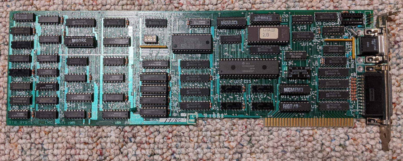
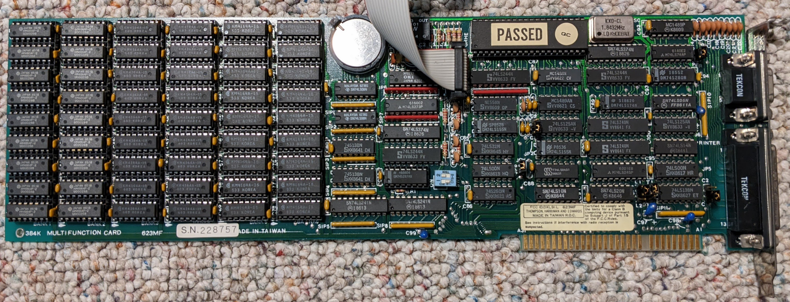
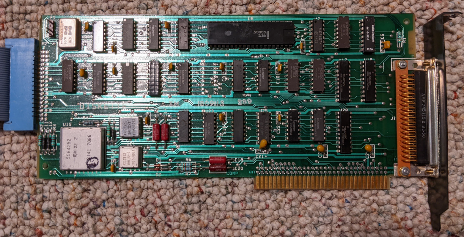
 
This trace is very impressive! I'm using an inexpensive ($12) 8-Channel USB logic analyzer with PulseView which isn't bad for free. I've applied a few decodes, but nothing this helpful! So at the moment I'm thinking how to do this trace in two steps, I'll have to see if PulseView has address decode, I'm sure it does.

8253_428.png
 
So at the moment I'm thinking how to do this trace in two steps
How about 3 captures:

1 = { /CS, /RD, /WR, two address bits }

At this point, you will be confident that /RD is not being asserted, and so drop it from the capture.

2 = { /CS, /WR, two address bits, upper nibble of data }
3 = { /CS, /WR, two address bits, lower nibble of data }
 
The 8253 came today so I installed it, looks like we're a lot further, time so start hooking more stuff up, and thanks for your help with this!! (speaker is beeping now too)

1677888526190.png

I've put the Cassette BASIC ROMS back in, but checks are still failing.

I also put the original BIOS ROM back in the board to see what it would do, I get:

0840 201
Parity Check 1

I see from your post here that indicates an error in Bank 2, bit 6 chip. Interesting that the Diagnostic ROM didn't find a memory error as well.
 
Last edited:
I've put the cassette ROMS back in, but checks are still failing.
Re the 8087 test. I see that switch 2 in switch block SW1 is set to ON, i.e. no 8087 fitted. A quick look at the source code for the diagnostics indicates that the diagnostic always expects an 8087 to be fitted. That is probably because the diagnostic can't trust that the reading of SW1 is good (everything is under suspicion). I see that the Supersoft/Landmark diagnostic will display "NOT PRESENT".

Re the floppy test. Is there a floppy in drive A: ?

Re the 'Check ROM at Fxxxx' tests. Their failure is the result of a bug in the 2022-12-12 version of the diagnostics. See the 'Known bugs' section of [here].

Put the IBM BIOS ROM back in.
 
Re the floppy test. Is there a floppy in drive A: ?
I haven't hooked up a floppy drive yet
Re the 'Check ROM at Fxxxx' tests. Their failure is the result of a bug in the 2022-12-12 version of the diagnostics. See the 'Known bugs' section of [here].
Oh, good to know!
Put the IBM BIOS ROM back in.
I swapped bit 6 chip & 7 in bank 2 and confirmed that memory chip is bad because now parity error is 0880 after the swap. Luckily I have a few extra 4116 RAM chips here from a TI-99/4A VRAM fix ;) Popped one in, and we're back in business!

1677891355292.png

Ok now to start fitting those cards back in the machine.
 
I have added your motherboard to the list at [here].
Cool, I hadn't seen that page before!

Here are the cards that came with the machine. Frankly I'm not sure which is the display card! (for troubleshooting I've been using the video card from a 5160)
  • IBM 64KB Memory Expansion Option
    • 0pdo5Ffk_Q8cMI54jmYt9nUQdCn5z2DRH8K5SSQBwGOfHaHxTmUKXgnRaPECNVXrNv49g1tme0g9iY9_x5hjXmUvNhKvCpQ5rDoH5FuMw2VdaM-U7acOcP22jhaMDmcIl77_MP8jsGar389yG2ciVjU
  • STB “The Chauffeur”
    • T8bu62TUuvZJ6tg5lhRO2ah2cPQl-zdxHGihLK4UL0isqVlkfIbyfXFR45JJRUXcG_Nq_uKZ09Xmntg98450TMYPpKwN73ZOwIuWJhDD1CLw9cZ0SKdgMNgThb-ZPNqbcw-xMjIE2zeKrGdPpAHiNqk
  • Multifunction Card??
    • 5CQiEgE-6migUyxa7Ugl_OYLmgJOE0Da4ovaowWU2NaP8cyaXMuApQzebf9bz_oYaE8aDqCIQOzb_Zv1ekCiPdTI4JRyEpvy_cjTg1jhzxPgn5mqYAg-gAO0EZuZrQeOo-r8pMGJ79kCqUZSBCyrlA4
  • IBM 5.25" Diskette Drive Adapter
    • F0Y5O44EuM6FoAbNHWTK9m7_Oxzk_V0_8ei-OxzsX3s3-VdsGXAOPpFGHH0MfUeYCBST6q9R1DDID7-bxtgb3cGxH4nbJom4PjgEL2L-VyOe6ZJfxcT2XUvicxhBebzC2bicKWkaRRkDuuZuKttMpvI
 
Multifunction Card??
Yes.

1677892654464.png

In the FCC ID, 'DXL' is a code for the maker.
DXL = Lung Hwa Electronics Co. Ltd.
Maybe 'Thompson, Harrman and Edwards' had Lung Hwa make the card for them.

Note the '623MF' bit, something that is also printed elsewhere on the card (left of the serial number sticker).
That is sure to be the model number, with the 'MF' bit being short for multi-function.
 
Re the 623MF multi-function card:

• RAM.
• A real-time clock (RTC) based on the Oki M5832 chip, backed up by the battery.
• A serial port (the male DE-9 connector).
• A parallel port (the female DB-25 connector).
 
Re the 623MF multi-function card:

• RAM.
• A real-time clock (RTC) based on the Oki M5832 chip, backed up by the battery.
• A serial port (the male DE-9 connector).
• A parallel port (the female DB-25 connector).
Good stuff, I'll have to take advantage of those ports!

I have the motherboard fitted back in the chassis, tested the Chauffeur and it's working. Starting to piece things together.
 
The switches on the IBM 64KB Memory Expansion Option are configured to start the its RAM at address 64 KB.
So, the RAM story should be:

Addresses 000 to 064 KB: 16KB-64KB motherboard
Addresses 064 to 128 KB: IBM 64KB Memory Expansion Option
Addresses 128 to 512 KB: 623MF card (6 banks of 64 KB = 384 KB)

The address range quoted above for the 623MF card is presumed (due to no documentation so far).
 
I expect that the parallel/printer port on the Chauffeur uses I/O base address 3BC hex, just like the IBM Monochrome Display and Printer Adapter.

The parallel/printer port on the 623MF card is probably using 378 hex.

If so, DOS will assign 'LPT1' to the port at 3BC hex, and will assign 'LPT2' to the port at 378 hex.
That is different to what card makers and diagnostic software typically use for LPT1 and LPT2 - see post #4 at [here].
 
I expect that the parallel/printer port on the Chauffeur uses I/O base address 3BC hex, just like the IBM Monochrome Display and Printer Adapter.
The parallel/printer port on the 623MF card is probably using 378 hex.
If so, DOS will assign 'LPT1' to the port at 3BC hex, and will assign 'LPT2' to the port at 378 hex.
That is different to what card makers and diagnostic software typically use for LPT1 and LPT2 - see post #4 at [here].
Thanks for that, once I get it all back together I'm going to look and see what diagnostic software can test these things. Maybe Check-It and InfoSpotter?

A few extra notes:
  • The memory expansion card was shorting out the power supply. Replacing two tantalum caps on the board remediated that.
  • When I fitted the multifunction card I had a 5040 201 memory error. After a little spread-sheeting + trial and error figured out that bank 1 = 20, bank 2 = 30, bank 3 = 40 etc. I scavenged a 4164 out of a Compaq portable motherboard I have floating around and it came up clean
  • Successfully booted into DOS 6.22. The Mitsubishi floppy drives are a little on the noisy side but work well.
  • Took apart the power supply and blew the dust out with compressed air. I was checking to see if there were any RIFA caps in there (the kind that burn up and smell) but I didn't see any. Other than normal dust it looked clean in there.
 
I see from your post here that indicates an error in Bank 2, bit 6 chip. Interesting that the Diagnostic ROM didn't find a memory error as well.
Yes, interesting. I have added investigation to my to-do-list.
I brought out a 5150 motherboard of type 16KB-64KB. I removed the bit 6 chip in bank 2. I powered on the motherboard and, as expected for that motherboard type, saw 0840 201.

I then substituted the 2022-12-12 version of Ruud's Diagnostic in place of the IBM BIOS ROM. I powered on the motherboard and, as expected, Ruud's Diagnostic indicated a bit 6 problem at 32 KB.

So, perhaps your faulty bit 6 chip was intermittent.
 
Thanks for that, once I get it all back together I'm going to look and see what diagnostic software can test these things. Maybe Check-It and InfoSpotter?
The POST records what ('standard') serial and parallel ports it found, and records those in the BIOS Data Area. You can use DEBUG to see those - see [here].

Yes, diagnostic software like CheckIt can test the ports. For such software to fully test them requires loopback plugs (one for serial and one for parallel). Information on the serial loopback plug is included at [here].

Be wary of what information that CheckIt (and others) report. For example, at [here], I have started to compile wrong/misleading information that CheckIt versions 2.1 and 3 display.
 
Back
Top