Christoffer
Experienced Member
Hi! so, i'm currently messing around with a small "ECB" z-80 computer i bought. I think it's a swedish traffic data controller from the 80's, from the ascii strings i can see in ROM.
The CPU card is a true SBC, with 4K rom, some SRAM, Z80 CPU, Z80 SIO/2, and Z80 CTC (that also sets baudrate).
it boots, then stays on boot message forever. If a key is held down during boot, or if the accompanying RAM/ROM card isn't inserted it goes to a monitor style promt or debugger where you can edit memory, see registers and run from address etc. it has a few options i've no idea what does too.
All the boards look non-specific built, so it SHOULD be possible to get it running other stuff (BASIC, CP/M even.), but there's one problem: A lot of the decode is done in 82S131 PROMS which I can't read, so I can't directly find the address for the UART and CTC hardware wise.
Also, the RAM/ROM card has a full 64K SRAM/EPROM mix, so the CPU card MUST be able to switch between memory on card/memory on bus. This could be a flipflop set via an IO address too i suppose.
Question is how do I figure these hidden addresses out? My plan was to look at the small 2K roms on the CPU card, since these must have routines for serial, and so the hardware addresses should be declared somewhere presumably in the start of the code, i'm just not smart enough to decipher disassembled code.
Here's the first bits of code, and the first use of "OUT", which I assume is what i'm looking for.. Any ideas?
Thanks in advance!
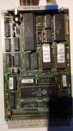
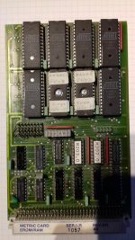
oh, and here's a few pics of the boards.
The CPU card seems to be from JET computers AB, memory from "Metric"..


The CPU card is a true SBC, with 4K rom, some SRAM, Z80 CPU, Z80 SIO/2, and Z80 CTC (that also sets baudrate).
it boots, then stays on boot message forever. If a key is held down during boot, or if the accompanying RAM/ROM card isn't inserted it goes to a monitor style promt or debugger where you can edit memory, see registers and run from address etc. it has a few options i've no idea what does too.
All the boards look non-specific built, so it SHOULD be possible to get it running other stuff (BASIC, CP/M even.), but there's one problem: A lot of the decode is done in 82S131 PROMS which I can't read, so I can't directly find the address for the UART and CTC hardware wise.
Also, the RAM/ROM card has a full 64K SRAM/EPROM mix, so the CPU card MUST be able to switch between memory on card/memory on bus. This could be a flipflop set via an IO address too i suppose.
Question is how do I figure these hidden addresses out? My plan was to look at the small 2K roms on the CPU card, since these must have routines for serial, and so the hardware addresses should be declared somewhere presumably in the start of the code, i'm just not smart enough to decipher disassembled code.
Here's the first bits of code, and the first use of "OUT", which I assume is what i'm looking for.. Any ideas?
Code:
				;
				;	Disassembled by:
				;		DASMx object code disassembler
				;		(c) Copyright 1996-2003   Conquest Consultants
				;		Version 1.40 (Oct 18 2003)
				;
				;	File:		DADACmout.bin
				;
				;	Size:		2048 bytes
				;	Checksum:	D5EB
				;	CRC-32:		9BCF39D4
				;
				;	Date:		Sun Jun 03 20:04:13 2018
				;
				;	CPU:		Zilog Z80 (Z80 family)
				;
				;
				;
					org	00000H
				;
0000				L0000:
0000 : 18 08		"  "		jr	L000A
0002 : C3 97 00		"   "		jp	L0097
0005 : 18 F9		"  "		jr	L0000
0007 : C3 4B 01		" K "		jp	L014B
				;
000A				L000A:
000A : 31 00 13		"1  "		ld	sp,01300H
000D : 21 00 10		"!  "		ld	hl,01000H
0010 : 11 01 10		"   "		ld	de,01001H
0013 : 01 FF 02		"   "		ld	bc,002FFH
0016 : 36 00		"6 "		ld	(hl),000H
0018 : ED B0		"  "		ldir
001A : 3E 12		"> "		ld	a,012H
001C : ED 47		" G"		ld	i,a
001E : ED 5E		" ^"		im	2
0020 : 21 07 05		"!  "		ld	hl,00507H
0023 : 22 F4 11		""  "		ld	(X11F4),hl
0026 : 7D		"}"		ld	a,l
0027 : 21 06 01		"!  "		ld	hl,00106H
002A : 18 10		"  "		jr	L003C
				;
002C : 00		" "		nop
002D : 00		" "		nop
002E : 00		" "		nop
002F : 00		" "		nop
0030 : 00		" "		nop
0031 : 00		" "		nop
0032 : 00		" "		nop
0033 : 00		" "		nop
0034 : 00		" "		nop
0035 : 00		" "		nop
0036 : 00		" "		nop
0037 : 00		" "		nop
0038				L0038:
0038 : F3		" "		di
0039 : C3 F1 05		"   "		jp	L05F1
				;
003C				L003C:
003C : 11 00 12		"   "		ld	de,01200H
003F : 01 20 00		"   "		ld	bc,00020H
0042 : ED B0		"  "		ldir
0044 : 21 D4 00		"!  "		ld	hl,000D4H
0047 : CD C9 00		"   "		call	L00C9
004A : E5		" "		push	hl
004B : 21 00 11		"!  "		ld	hl,X1100
004E : 97		" "		sub	a
004F : 77		"w"		ld	(hl),a
0050 : CD C3 00		"   "		call	L00C3
0053 : 3E 30		">0"		ld	a,030H
0055 : ED 79		" y"		out	(c),a
0057 : 18 11		"  "		jr	L006A
Thanks in advance!
oh, and here's a few pics of the boards.
The CPU card seems to be from JET computers AB, memory from "Metric"..
