Okay, Christmas break with family is now over, so getting back to the computers.
So it looks like there are 3 paths I can take to trace the VDU circuit board.
Path 1: start at edge connector.

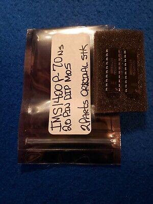
Path 2: start at SRAM chip. I assume that means U62-U69.
Path 3: start at the MC6845 chip.
I chose path 3 first, starting at the MC6845 chip since it gave me a single starting point, specifically pin 26, and sounded like it would fork the least.

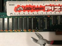
Here are good photographs of the front and back of the VDU board. I started by printing these out on paper and then using a red ink marker to literally trace the traces I was finding. I should have continued doing that, but I stopped it at some point and will have to catch up on it, or redo it since it the marker writing got too hard to read. This allows me to write down what physically leads to what.


In parallel to the red ink tracing, I started writing a "trace flowchart" on a separate piece of paper. This allows me to write down in words what leads to what. Here is my paper on that so far, aided critically by looking up data sheets on the chip numbers.

The network forks out several times as I follow is from MC6845 pin 26.
Thank you for the link. The schematic pack has schematics for 3 different versions of the VDU, on PDF pages 63-81. I looked through all of them but I don't see anything marked "video RAM" or similar or "U62" through "U69." Again, this is the first time I've ever tried to read a schematic, so please tell me if I missed it in there.Although this is the 286 Technical Reference, the Video Display should be effectively the same between the Portable and Deskpros: https://onedrive.live.com/?authkey=!AJOmtRmVhlhL6_o&cid=7D567B5161FE0EB7&id=7D567B5161FE0EB7!47144&parId=7D567B5161FE0EB7!37014&o=OneUp
So it looks like there are 3 paths I can take to trace the VDU circuit board.
Path 1: start at edge connector.
With the equipment you have the easiest way is start at the edge connector. If you look online at the pinout data 7 is B2. Follow the trace from that pin to a chip or it may go to multiple chips. If you can't follow the trace you will need to start checking with your meter on beep to see where it goes. If you get a beep check with ohms and verify its really close to 0 ohms.
Path 2: start at SRAM chip. I assume that means U62-U69.
Also can start from the SRAM chip data pins Check the chip datasheet and find the same bit on the "other side" of the chip. D7->Q7, A7->B7 etc. Follow that signal until you get path from SRAM to connector. The SRAM chip uses separate pins for data output and input on 8 and 12. You want to trace to one of those pins.
Path 3: start at the MC6845 chip.
It may be simpler to trace to the MC6845 data pins since we know which D7 (pin 26) must be for the board to function. Likely less layers of chips to trace through than to edge connector. This will be time consuming. I can look some at my board if you get stuck.
I chose path 3 first, starting at the MC6845 chip since it gave me a single starting point, specifically pin 26, and sounded like it would fork the least.
Here are good photographs of the front and back of the VDU board. I started by printing these out on paper and then using a red ink marker to literally trace the traces I was finding. I should have continued doing that, but I stopped it at some point and will have to catch up on it, or redo it since it the marker writing got too hard to read. This allows me to write down what physically leads to what.
In parallel to the red ink tracing, I started writing a "trace flowchart" on a separate piece of paper. This allows me to write down in words what leads to what. Here is my paper on that so far, aided critically by looking up data sheets on the chip numbers.
The network forks out several times as I follow is from MC6845 pin 26.
- Does this trace flowchart look sound so far?
- Are there forks where I should cease tracing, and instead go down others? If so, which to not bother with and which to definitely continue?
- Is I0 the correct pin I want to go out from at SN74LS151NDS? Here is the pinout.

Last edited: