• Please review our updated Terms and Rules here

Help on monitor issue with Taxan 770 plus, powers on but video collapses.

This service manual is weird. There are two revisions maybe? Page 78 of the PDF has C1524 listed as 2.2uf 50V which is what was there at the location. I can try and find original pictures to confirm if I happened to catch that area.

I have also noticed quite a few discrepancy's between the parts lists and the values on the schematic, but it always seems so far one or the other is always correct. I can say there is no rhyme or reason. Sometimes the schematic is right, sometimes the part list manifest is right when matching up what is actually there.
 

Attachments

  • c1524.png
    c1524.png
    201.5 KB · Views: 4
Last edited:
Found a picture from before the recap of that area. You can just make out a 2.2 on the cap...
 

Attachments

  • 20230220_230048.jpg
    20230220_230048.jpg
    1.4 MB · Views: 5
  • 20230220_230048-edit.png
    20230220_230048-edit.png
    1.1 MB · Views: 5
... then that cap is ok and not the problem.

We need to find another voltage source to power the H output stage, or find away to lower the voltage, so we can test the control loop without the EHT being high and initiating shutdown.

Do you have any variable DC power supplies ?

Do you have any assorted parts such as silicon NPN power transistors ?

Can you check if the ripple filter transistor Q1905 in the power supply is on a heatsink ?

Do you have a function generator, we could try to drive Q1502 from another source to get the output voltage closer to 50V.
 
Last edited:
I don't have any variable DC supplies. All I have is assorted wall wart adapters mainly in the 12-24 and a few 48v power supplies from a POE switch, etc.

I have a few NPN transistors, and I can report a bit later with what I have, but I am happy to place an order for any that is suspect. Just let me know and I will get them on the way.

Q1905 is to the right of 1502, so there is the heatsink behind it, however there is nothing to clamp or hold it to the heatsink, so there is a mm or so gap. You want me to try and get it pushed up and stuck to the HS with some thermal paste?

I have a BK 3020 sweep/function generator. Also have a HP 8640b signal generator if that helps, but figured that is more on the side of radio gear.
 
If we supplied a 50% duty cycle 15kHz square wave, from a function generator to transistor Q1513 (after disconnecting its base drive from the feedback loop), the drive to the buck regulator and Q1502 (if that part of the system was working) would be such that its output would likely be between about 50 to 60V, this would probably produce a sensible scan width and moderate EHT, without triggering the protection circuit. Then we could test the rest of the feedback loop. (Often if something is wrong inside a feedback loop, the loop has to be disconnected, to find the fault)

I'll see if I can find the manual for the function BK generator. If the generator can produce a few volts is all that is required

The other option is to make an analog regulator, that will drop the 125V down to around 50V, though doing it that way, the pass transistor would have to be on a substantial heat sink, so it would have to be an external device added to do the experiment.

I'm pretty sure the buck regulator is working though, even though the output voltage is too high. The reason being, its a switching regulator. If the switching stops, the output would be zero (unless the transistor was shorted or incorrectly installed). It is just that the duty cycle of the switching must be incorrect. So, likely I suspect, the problem is in the region of the OP amp or prior to that, where the pulse amplitude from the flyback is sampled, or after, when the signal is gated through.

In the meantime can you check that Q1502 was correctly re-installed.
 
If we can get the buck regulator running with a sensible output voltage and the VDU stable and not under threat from over-scan and over EHT voltage, part of diagnosing it is going to be to figure out how the AN6558 OP amp has been configured to work for the task.

This regulator has a fairly fast correction response time, I see that they injected a pincushion correction voltage onto the adjustment pot.

The first op amp compares the voltage derived from the H output transformer (after peak rectification) to the zener reference, pin 5 & 6, it is acting as a comparator and an integrator (on account of that 2.2uF bipolar cap) then the level out of it, pin 7, is used to gate through the H pulses in the other OP amp in the package. For this to result in a variable duty cycle pulse though, the H pulses that are derived from the HA11235 would have to be in the form of a ramp or sawtooth.

In any case if we can get the VDU running and stable and the buck regulator itself is ok, scoping pins 7 and 1 of the AN6558 OP amp will probably show what is wrong.
 
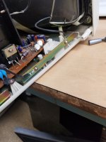
I have been pondering the best way to get on with this repair. If the VDU was in my lab I would have connected the H output stage to a variable DC supply. But we don't have that luxury.

One way to reduce the voltage to the H output stage would be with an appropriate value power resistor, but it is hard to calculate the Ohms value and the required power rating, because we don't know the current consumption.

So I have come up with an idea, perhaps a little unorthodox, but I think it will work, if you are prepared to splash out $20 or so on a part.

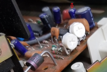
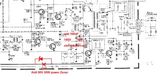
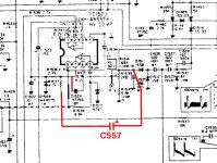
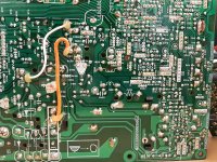
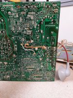
The idea is to cut the B+ feed to the H output stage and fit a Power Zener diode in series. If we use a 50W rated part, and screw it to a reasonable sized chunk of metal, say about 6 x 6 inches approx or more, it will handle the power. You can run a couple of wires to it and have it a foot or more away from the VDU, it will run quite warm I would expect. I would recommend adding some additional capacitance as indicated, you can tack a spare 100uF 160V cap across the 10uF that is there.


This will knock 50V off the supply voltage to the H output stage and I think will bring the EHT down, to likely in the range of 18 to 24kV , and allow the VDU to run without the shutdown deploying and at least in a safe enough condition not to get a high voltage related failure, while we are trying to figure out what has happened. Certainly if this prevents the shutdown, the EHT voltage will be in the range the manufacturers thought the circuitry could tolerate.

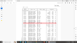
The best estimates we can make currently is that the EHT is about 8.2/5.6 (the OP amp voltages for the shutdown circuit, the normal being 5.6 and you measured 8.2) or about 1.46 times over the level that trips the shutdown, or also roughly 34/24 or about 1.4 times what it should be, if we assumed that the usual EHT was around 24kV. The buck regulator probably is running at its max duty cycle (if a shorted transistor is excluded) and I'd expect at least 110V out of it (not the full 125 as it has to be in a switching mode). So likely if we reduce that output by 50V, the supply to the H output stage will be around 60V, which should be ok, but the exact value depends on what the buck supply is putting out in this fault condition. I wouldn't recommend trying to check that by deactivating the shutdown again, that would be pushing our luck.

In addition, if the 54V at the emitter of the buck transistor, is the value that is normally there in the scan mode where it was tested with the shut down deactivated, then we can deduce that likely the 54V is about 54 x 1.46 = 78V at least. in this case we would in fact have to only knock 25v or 30V off it. So I think the 50V reduction will be more than enough. Though we could always move to a lower voltage zener. We can always measure the voltage if the VDU stays running.

Then, we will be able to scope the OP amp and buck regulator circuit and find out what has gone wrong.
 

Attachments

  • Zener.jpg
    Zener.jpg
    314.4 KB · Views: 5
Last edited:
So will the BK 3020 work for this application you think? Also you talk about needing about 50-60 volts, do you think the 48-56 volt power supply (150Watt) supply from a POE switch would work?

Otherwise I have a dozen or so 2sc2625 and assorted IC's off 3 or 4 more modern CRT's that were saved for parts.

If not do you think pin 7 and 1 would require much time we could try to risk again to power up the circuit if I don't have the means to inject a wave and find suitable voltage for the system.

I took the rubber boot off and checked Q1502 (C3336) across the emitter and collector while in circuit.(it didn't have a short when it was pulled and tested a month or so back). I get 3.8K one direction and 404.5K with the probes swapped. The part to the right is Q1905 and both transistors appear to be correctly orientated.

EDIT>>> Just saw you posted an additional option while I was typing. Looking now...
 

Attachments

  • 20240205_201410.jpg
    20240205_201410.jpg
    1.1 MB · Views: 3
  • 20240205_201435.jpg
    20240205_201435.jpg
    947.9 KB · Views: 3
  • 20240205_201446.jpg
    20240205_201446.jpg
    1.6 MB · Views: 3
Also you talk about needing about 50-60 volts, do you think the 48-56 volt power supply (150Watt) supply from a POE switch would work?


EDIT>>> Just saw you posted an additional option while I was typing. Looking now...
A 48 to 56 volt DC 150W rated supply would likely be ok, if you have that, simply make the cut in the feed I suggested where the zener might go, and power the H output stage with that. When you do it, switch on the VDU first, then switch that added power supply on. Make sure to observe the polarity.

If the VDU runs without shutdown, initially measure the voltage out of the buck supply (voltage across C1533), and we will find out how high it was.

As I mentioned, I don't think we should deactivate the over-voltage protection system again, it is too risky for the VDU.
 
Was testing a few other transistors and I noticed Q1511 was shorted between base and emitter. I took the transistor off and the short is not on the transistor. Following down to the transformer it seems strange on the loops and wanted to make sure this was normal. Pin 5 + 8 gives me 3.4ohm, pin 3 + 4 gives 0.19ohm, but pin 1 + 2 is open. Wanted to make sure there wasn't something wrong with pin 1 + 2. Looks like the Wire W120 was what joined the base and emitter together, but still seemed strange that pin 1 and 2 showed open. Looking at the schematic it looks like 1 and 2 are not even on there, so maybe these are extra unused coils?
 

Attachments

  • 20240205_225307.jpg
    20240205_225307.jpg
    2.8 MB · Views: 6
A 48 to 56 volt DC 150W rated supply would likely be ok, if you have that, simply make the cut in the feed I suggested where the zener might go, and power the H output stage with that. When you do it, switch on the VDU first, then switch that added power supply on. Make sure to observe the polarity.
If the VDU runs without shutdown, initially measure the voltage out of the buck supply (voltage across C1533), and we will find out how high it was.

If the Zener would be a more direct and safer bet I don't mind to get it. I am pretty sure I have a 3x6" aluminum heat sink somewhere around here. If we used the 48-56v supply the zener wouldn't be needed, correct? I just don't want to hook something up backwards or turn it on in the wrong order. If you wouldn't mind to double check I have it connected correctly before power on I don't mind to use the PoE supply I have. Otherwise let me know and I will order the part you linked.
 
If the Zener would be a more direct and safer bet I don't mind to get it. I am pretty sure I have a 3x6" aluminum heat sink somewhere around here. If we used the 48-56v supply the zener wouldn't be needed, correct? I just don't want to hook something up backwards or turn it on in the wrong order. If you wouldn't mind to double check I have it connected correctly before power on I don't mind to use the PoE supply I have. Otherwise let me know and I will order the part you linked.
OK, the safest thing (for the VDU) to do, would be to use the zener method, it certainly cannot do any harm.
 
PS: we know that the H output transistor Q1511 and its driver circuitry is fine, if there was a problem there, there would have been no scan and no EHT. Often when people test H output transistors in circuit , it looks like the B-E is shorted because of the very low DC resistance of the transformer driving the B-E circuit.The B-E is driven by pin 3 & 4 of the transformer (via the wire link). Pin 1 +2 do not appear to be used and they are not documented on the schematic.

I mentioned before, don't pull out random parts for testing, just in case another issue gets accidentally introduced. We really only want to pull out a part if we have some evidence it is defective. For example, if you made an error re-installing it, and we move to the next experiment or test, it would completely confound the results. We only want to do one thing at a time, and do tests in between. In many ways this is how things can go wrong with jobs like a global re-capping. Ideally, as each cap is replaced, the VDU (or whatever it is) is re-tested, so if a problem gets introduced after a part change or re-fitting, you know where it is.

(Also make sure that the heatsink clamp and insulation is re-fitted to the power transistors seen in post #88 which were removed for that photo, if that is left off their junctions will over heat later when the VDU is re-powered).
 
Last edited:
Got it. I will reassemble and wait for the diode that has been ordered. Hopefully will have it by this weekend.

Thanks..
 
Got it. I will reassemble and wait for the diode that has been ordered. Hopefully will have it by this weekend.

Thanks..
Before the diode is fitted, with the unit back to its normal state (although faulty) we need to test it again briefly, to see if it is still behaving exactly as it was, with a start up then a self shutdown, just to make sure nothing has changed after the removal and re-fitting of the H output transistor and heatsink/insulation etc.

It shouldn't take too long, after we get the VDU running with the Zener, to find out what has gone wrong with the voltage regulator.

Basically the design is a pwm controller, the output of the OP amp (on pin 1 of the AN6558) on account of a sawtooth voltage on one input terminal (at horizontal scan rate) and a DC control on the other, and running in open loop mode (very high gain) produces the pwm signal that drives the input transistor Q1513, on the three transistor driver, which drives the transformer for the buck pass transistor Q1502. As you can see they AC coupled that signal with capacitor C1523, and then DC restored it with diode D1503. The reason they did this, it that if the pwm signal stops (for example shut down), the voltage at Q1513's base goes to zero, so the driver transistor Q1503, directly on the transformer also cuts off, so it is not left with a high direct current via the transformer primary .

One curio is that C1522 is drawn on the schematic as an electrolytic cap. But its a 0.01uF in value and listed as that on the parts list, this is not a value that a electrolytic cap normally comes in.

In the meantime, can you post a photo of the track side of the pcb in the region of the AN6558.
 
Last edited:
Now that we have a good idea where the problem is, I'd do a quick in circuit check of the parts around IC1503 (particularly pins 5, 6, and 7). Don't remove anything unless it measures suspiciously. If anything is blocking the signal from pin 10 of the flyback it would lead to excessive HV. You're looking for something obvious like a shorted diode, open resistor, damaged circuit board trace, or solder bridge.
 
Here is the corner section you requested. IC503 is the AN6558.

Andy..
Thanks for the tips. Will try and take a look at the area later this evening.
 

Attachments

  • 20240207_164751.jpg
    20240207_164751.jpg
    2.1 MB · Views: 5
Last edited:
I spent about an hour last night taking measurements of diodes and resistors and I just can't seem to find anything that jumps out at me. I thought I had something when R521 read 0.10 ohms no matter how I turned the pot, but when I reversed to the other end it worked normally. The HV ADJ (R539) did the same thing, so figured that was the way it was suppose to be.

All the parts are soldered back from when I pulled the H OUT Transistor. I will get it reassembled tonight and do a power test before the zener comes. Looks like it is about 2 days away.
Can you take a photo of the pcb tracks in the region of the flyback transformer to include pin 10 and the track leading from there all the way to the high voltage adjust circuit where the AN6558 is.

One thing we need to be prepared for, fault finding this circuit, is that the schematic in the area is not correct, in that it does not match the pcb (See attached). There is also an additional resistor I think.

What does the parts list say about C557 ?
 

Attachments

  • Taxa.jpg
    Taxa.jpg
    96.1 KB · Views: 4
Last edited:
I can take a more specific photo tonight when I get home if this one that was already on my phone won't work. Let me know..

C557 shows on the parts list as 10uf 160v. There are a few spots on the PCB where factory work had been done with a diode and several other components that had legs soldered together on the top part of the PCB. I can take pictures of that as well.
 

Attachments

  • pin10.jpg
    pin10.jpg
    4 MB · Views: 5
  • 20231127_190123.jpg
    20231127_190123.jpg
    2.5 MB · Views: 5
Back
Top