• Please review our updated Terms and Rules here

how do logic ICs handle oscillating data?

tezza

Veteran Member
Joined
Oct 1, 2007
Messages
4,731
Location
New Zealand
This is a newbie question but I’ve tried to google an answer without success. I know some of you guys will know the answer to this straight off.

I’m mystified how logic ICs work with digital circuits carrying data? I know the principles of these ICs work i.e. how H or L inputs determine a certain output (either H or L) but what happens when a oscillating wave is used as input, as you would get in a computer circuit carrying data.

I’ve always assumed if a wave was used as an input, the output would also be a wave? If could be inverted or changed by other inputs but it would always be a wave. After all a wave is just a circuit oscillating between H and L except many times a second.

However recently I’ve been using an oscilloscope for diagnostic purposes and have discovered my assumption may be flawed. Take a TC40H139P IC. This is a dual decoder/multiplexer. Where a wave appears on ENABLE, or INPUT A or B, I would have expected a wave on all Y0-3 outputs? The exception being if ENABLE is steady H, in which case it doesn’t matter what A and B is, it will always be H.

This is not the case. When there is a Wave on either ENABLE, A or B, some of the outputs are a steady H and some are waves? I don’t know how to interpret truth tables with signals that carry a wave. I’d always assumed the signal would be flicking back and forth between H and L and the output would usually do so as well unless the truth table says it’s forced into a H unconditionally, by another input. This doesn’t always seem to be the case though.

Is someone able to explain it to me?

Tez
 
I'll take the first shot .. the TTL standard voltage levels for logic inputs separate the L from H sufficiently to avoid ambiguous data, something like 0-2.5 V = L and 3.5 - 5.0 = high.
If the "wave" is a clean square wave, generally no problem, if anything else you would use an IC with a Schmidt trigger input to clean it up first. The inputs and outputs of simple TTL logic chips are only intended to be H or L, hence the term "logic ICs." They can run at very high speeds so generally have square wave inputs and a square wave outputs - outputs being conditional on the specific function of the chip.

If you can get a hold of a 70's orange Texas Instruments TTL catalog it is full of useful information.
 
Last edited:
Thanks Paul,

Maybe my "logic chip" definition is too narrow. The chip that started me wondering on all of this was a TC40H139P IC dual decoder/multiplexer IC. If has ENABLE and A and B as input and Y0 to Y3 as outputs. The waves coming in and out are of the system I'm loooking at are not clean square waves generally.

I have to race off and do some Xmas things right now but thanks for your answer. Any other comments welcome.

Tez
 
I’ve always assumed if a wave was used as an input, the output would also be a wave? If could be inverted or changed by other inputs but it would always be a wave. After all a wave is just a circuit oscillating between H and L except many times a second.

No, this only true if the wave (clock signal) is 'gated' on. It can be 'gated' off when necessary.

Look at a 2 input AND gate. When one input is high, the other input is 'gated' on and passes to the output. If one input is low, the other input is 'gated' off and the output is a steady low.

Study the truth table of a AND gate and it will be clear how they gate signals on and off.

Input1 0101
Input2 0011
Output0001

Assume IN #2 is a control signal. When it is low (first two columns), the output is low no matter what IN#1 is doing. But when IN#2 is high, IN #1 is gated through and the output follows IN #1.
-Dave
 
This is a newbie question but I’ve tried to google an answer without success. I know some of you guys will know the answer to this straight off.

I’m mystified how logic ICs work with digital circuits carrying data? I know the principles of these ICs work i.e. how H or L inputs determine a certain output (either H or L) but what happens when a oscillating wave is used as input, as you would get in a computer circuit carrying data.

I’ve always assumed if a wave was used as an input, the output would also be a wave? If could be inverted or changed by other inputs but it would always be a wave. After all a wave is just a circuit oscillating between H and L except many times a second.

However recently I’ve been using an oscilloscope for diagnostic purposes and have discovered my assumption may be flawed. Take a TC40H139P IC. This is a dual decoder/multiplexer. Where a wave appears on ENABLE, or INPUT A or B, I would have expected a wave on all Y0-3 outputs? The exception being if ENABLE is steady H, in which case it doesn’t matter what A and B is, it will always be H.

This is not the case. When there is a Wave on either ENABLE, A or B, some of the outputs are a steady H and some are waves? I don’t know how to interpret truth tables with signals that carry a wave. I’d always assumed the signal would be flicking back and forth between H and L and the output would usually do so as well unless the truth table says it’s forced into a H unconditionally, by another input. This doesn’t always seem to be the case though.

Is someone able to explain it to me?

Tez
Hi
It sounds like it is working as expected. The '139 is used to steer the
waves ( as you call them ). Think of this logic as like pointing a water hose
into several open pipes( Y0-Y3 ). Inputs A and B select which pipe
to point to and the ENABLE tell you when to turn the flow on or off.
What the high outputs tell you is that those outputs are never selected
by any of the combinations of A, B and ENABLE.
I think the thought that there must be an output at all times is flawed.
A quick check of the truth table for the '139 should tell you that.
It is maybe better to try to think of a logic element as something
that evaluates inputs and then produces specific outputs at discrete
times. There is some time delay but it is usually small compared
to the time frames involved.
The fact that some output stays high just means that it never
has the right combination of inputs to make it change. This may or
may not be bad for the circuit you are looking at.
This is where a logic analyzer has an advantage over a simple
oscilloscope. Its primary disadvantage is that you need to connect
all those inputs to places you expect to need to see.
I guess the first thing to realize is that the inputs are not just simple
square waves. At particular times, they may be a 1 or 0 but when
they change can only be predicted by knowing what is generating them.
In a processor, there is generally an abundance of activity. Address
and data lines are constantly changing. Still, if you stop things at
any instance of time you'll see that only one thing is happening when
you combine all the address, data, control and clock signals.
The '139 is only sampling the two inputs A and B when the ENABLE
is valid. The rest of the time it blocks the activity of A and B. The output
off state just happen to be high.
A typical use of a 139 is an address decoder. It produces select signals
for several devices. The ENABLE signal is only valid during the time
when the inputs, A and B, are expected to be valid. A and B would
be the address lines from the processor. The ENABLE might be a
combination of clock, bank select, rd/wr or other control signal.
Dwight
 
Ahh I see.

But how does one know what is gated on and gated off in one of these ICs?

I can't find a mention specifically of "gating" on the spec sheets but there is a lot of info in them. For example here is the data sheet for the TC40H139 IC. Is that info in there somewhere?

Thanks

Tez

At the bottom of the first page is the truth table. It shows what combination
of inputs will cause which output to go to zero.
The H and L should be obvious. The * means that input could be H or
L but has no effect on the states of the outputs at that time.
I thought I'd add, the concept of off and on may mean H is off and L is on
or it may be H is on and L is off. It all depends on what the next device expects
on the wire coming in.
Dwight
 
Dwight,

Thank you for that detailed reply. What's more, I can understand it!

I now know why a scope doesn't replace a logic probe. Seems like you need both devices in the toolkit.

Tez
 
Just this week I was troubleshooting my college digital electronics final project at home, and realized that I desperately needed a TTL logic probe. :shock:

I had very limited supplies on hand, but I built one on a small breadboard with spare parts and finished my project on time.

You need a SN74LS06 inverter, a 470 ohm resistor (or close enough) and a red led. (and some wire) You power the chip with 5V on pin 14 and GND on pin 7. Pin 2 is connected to the 470 ohm resistor which connects to the cathode of the LED. the anode goes to 5V supply. Pin 3 is the logic probe input.

So if you need a TTL probe for a quick project, that's what worked for me in a pinch. Just in case that's helpful info.
 
Just this week I was troubleshooting my college digital electronics final project at home, and realized that I desperately needed a TTL logic probe. :shock:

The problem with the simple inverter logic probe is that it will only indicate a static high or low level. Add a one-shot to it to stretch pulses and you have a pulse indicator.

You can also have a bit of lighter loading by substituting a transistor instead of an '06. Or use a comparator.
 
That makes sense too. :) But that's just what I had on hand, and it worked. The only other chips I had were what I was using for the project itself. (Mostly comparators, each one a quad with all pins already in use) I also didn't have a transistor.

I had little more than what I had grabbed before I left the lab and only one night to finish the project. (Thanks to a good-for-nothing partner who literally didn't do a thing) The resistor and led were actually salvaged from commercially manufactured devices (just spare bits in my drawer that I kept). All the same, I got into the top three of the class. ;)
 
Last edited:
One point to make about the TC40H139P chip(or any TTL chip). Notice from the truth table that only one output is low at any given time. TTL chips draw more current both on the input and output when they are driven low than they do when driven high. If the logic values were reversed in the truth table the chip would draw significantly more current. Do you have a the "TTL Cookbook"? Good reference book with the rules of using TTL chips.
 
One point to make about the TC40H139P chip(or any TTL chip). Notice from the truth table that only one output is low at any given time. TTL chips draw more current both on the input and output when they are driven low than they do when driven high. If the logic values were reversed in the truth table the chip would draw significantly more current. Do you have a the "TTL Cookbook"? Good reference book with the rules of using TTL chips.
... except that this isn't a TTL chip, so any differences in current are really insignificant.
Even if it were, what's your point about "reversing" the truth table?
And yes, only one output (well, 0 to 2 actually) is active at any time because this is after all a dual "*one* of four" decoder; not sure what you're trying to say there either...

Sorry, should have noticed that this chip is CMOS. My point was to show that when designing logic circuitry with TTL chips, power consumption (and heat) need to be considered. In college I was taught that if a logic gate spent most of it's time in one state, it is better to make that state a logic high. The point was that would be the reason for the truth table being the way it is instead of reversed.

Edit: In college I was taught that if a TTL logic gate spent most of it's time in one state, it is better to make that state a logic high. The point was that would be the reason for the truth table being the way it is instead of reversed.
 
Last edited:
Tez,
Your choice of the spec sheet for the 40H139 dual 2 to 4 line decoder is a good one to study. Here is some info expanding on Dwight’s last message to help you understand the notation used in the truth table and circuit diagram as it can be confusing.

The inputs and outputs with a bar over their name are active LOW meaning when they are asserted to a low state, the signal will be considered ‘on’ or ‘true’. Confusing, right? Look at the enable signal called G bar (or G/). When it is HIGH (false), the entire decoder function is disabled so that Y0/, Y1/, Y2/ and Y3/ are all forced high (not active).

If, on the other hand, the chip had been designed for the outputs to be named Y0, Y1, Y2, and Y3, it would imply they are active HIGH, and under the condition of G/ being HIGH, the outputs all would have been forced LOW (not active).

Now look at the schematic. By the G/ input at pin 1, you see a small circle (bubble) at the first inverter? This again implies a low active input. On the outputs you see bubbles there too indicating low active outputs. This is an aid in troubleshooting control signals although some schematics on commercial equipment do not always use the correct notation.
-Dave
 
if a TTL logic gate spent most of it's time in one state, it is better to make that state a logic high.

Yes that is a good point. Another reason for low active control signals was the better noise margin in TTL gates in the high state. There would be less exposure to dreaded glitches from noisy power supplies, etc.
-Dave
 
To the already excellent explanations, I'll add a caveat.

Many engineers write their schematics with the logical devices represented by their function and not necessarily the way they're designed on the datasheet.

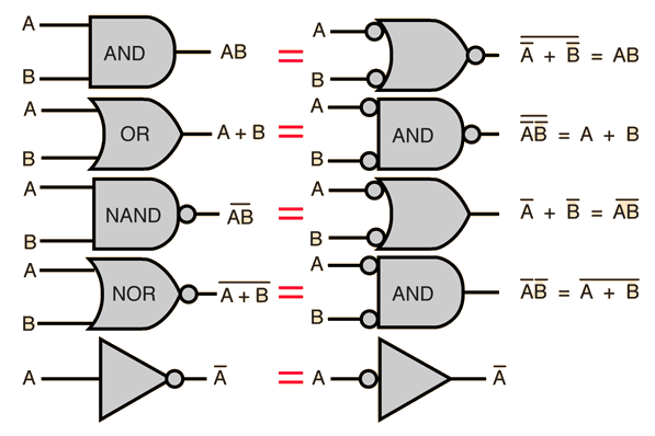
For example, if you go to your databook, you'll find out that a 74LS00 is a quadruple NAND gate. However, if the designer of the circuit is using negative logic he's likely to write the section as an OR gate with the inputs inverted (i.e. "bubbles" on the input lines). The truth table is the same (see De Morgan's laws), but the designer clearly wants to show that the inputs are low-TRUE and the desired function is the OR of these.

gate2.gif
 
Last edited:
For example, if you go to your databook, you'll find out that a 74LS00 is a quadruple NAND gate. However, if the designer of the circuit is using negative logic he's likely to write the section as an OR gate with the inputs inverted (i.e. "bubbles" on the input lines).

Chuck, yes excellent point. Good designers would do this on their schematics to help others to follow the logic flow. From a computer aided drawing (CAD) point of view, it was a little more trouble, but the guys troubleshooting broken boards later on would bless him for it.
-Dave
 
Guys,

I just want to thank you for those excellent explanations and examples. It's certainly aided my understanding not only of how this general class of ICs work but also in how to read the data sheets properly. That's very helpful.

Tez
 
Back
Top