• Please review our updated Terms and Rules here

How to Start hardware of 8085up......??

OK, I will use '138 then i have to connect A15 in such a way that when A15 is low then only memory decoder circuit will work. I am right??
Is it compulsory that the PROM addr should start at 0000H as it reset vector addr is at 0000h, so, can we change the PROM starting addr.???

and I think without RAM the program will not run as we need to store Stact, etc....
 
OK, memory decoder will work from '138 i have change my RAM addr. from 3000H to 4000H...!!
 
The 8085 uses its address lines to select up to 256 possible input ports and output ports. It puts out an 8 bit port address on its lower address lines along with an ALE strobe to allow the address to be captured. It also puts out the same 8 bit port address on its upper 8 address lines, and here the address is held through the transfer time. For that reason some designers prefer to use the upper 8 bits for selecting the I/O port. For this design, I chose to use the lower 8 bits since they are buffered by the latch. That way I don't have to worry about overloading the upper lines, or adding a buffer, if at some point down the road I add more memory devices to the system.
 
My post was incomplete..
I found this cool explanation of 8085 up, i think to read about 8085 self guide a good book must be there, which i don't have.

It also puts out the same 8 bit port address on its upper 8 address lines, and here the address is held through the transfer time. For that reason some designers prefer to use the upper 8 bits for selecting the I/O port. For this design,

I don't understand this, how A8 to A15 is used ?? for input output??
 
Okay, here's the way it works. Suppose you encode the following instruction:

LDA 1234H (stored in memory as 3A 34 12)

To perform the fetch, the 8085 gates 12H onto A8-A15 and 34H onto AD0-AD7 and asserts ALE. In the following cycle, the CPU de-asserts ALE and asserts RD and the memory device is expected to put the data found at location 1234H on AD0-AD7 in response. The CPU takes the data on these pins and moves it to the A register.

Now, suppose that the following instruction is executed:

IN 56H (represented in memory as DB 56)

The CPU places 56H on A8-A15 and 56H on AD0-AD7 and asserts ALE as above, but in the following cycle asserts IO/M (to show that this is an I/O read) and asserts RD as above. The I/O devices gates its data on to AD0-AD7 as with the memory example and the CPU moves the data to the A register.

One interesting side effect which is the subject of the Saundby's note is that the port address remains on A8-A15, during the I/O operation, which can be convenient for some applications.

Note that not all x80 family CPUs do this; for example, the Z80 behaves in a very different way.
 
I don't understand this, how A8 to A15 is used ?? for input output??

What's not to understand? What he's saying is that when you use the port input/output instructions on the 8085 the same 8-bit port address appears on both the lower (A0-A7) and upper (A8-A15) address lines, and thus you have the option of using *either* set of address lines to decode your 256 possible I/O ports addresses.

(In principle I could see the advantage of using the upper ones. Let's say you designed a minimal 8085-based embedded computer using the 8085-specific companion memory parts that include a built-in latch to demultiplex data from the lower shared half of the address bus. But it turns out you need use an I/O chip *without* the built-in latch. You could slightly simplify your bus decoding circuitry by landing it on the top 8 address lines and just treating the bottom multiplexed eight as data-only. That eliminates the need for an external address latch as long as you don't depend on the "data" lines containing *valid* data until the proper part of the transfer cycle.

If that all flew right over your head than I'd strongly recommend using a CPU without a multiplexed address bus for your first computer. Unless there's some external reason you're stuck with the 8085...)
 
(In principle I could see the advantage of using the upper ones. Let's say you designed a minimal 8085-based embedded computer using the 8085-specific companion memory parts that include a built-in latch to demultiplex data from the lower shared half of the address bus. But it turns out you need use an I/O chip *without* the built-in latch. You could slightly simplify your bus decoding circuitry by landing it on the top 8 address lines and just treating the bottom multiplexed eight as data-only. That eliminates the need for an external address latch as long as you don't depend on the "data" lines containing *valid* data until the proper part of the transfer cycle.)

Yep, and I used such a scheme for my 8085 SBC's expansion connector. It reduces the bus lines needed by 8, but since I included the ALE line, you can still decode all 16 address bits. Since there's 64K of memory on the SBC, a system with only I/O functions on the add-on boards benefits from a smaller number of bus lines /and/ it doesn't need another 8-bit latch. Handy when everything is on a 3x4" PC board!
 
Ok, then what the use of both same addr found in lower and higher addr lines??
 
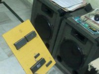
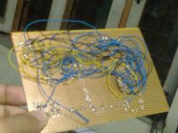
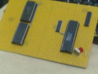
Till now i have assembled 8085 this much....
 

Attachments

  • 10092011119.jpg
    10092011119.jpg
    82.1 KB · Views: 1
  • 10092011118.jpg
    10092011118.jpg
    85.3 KB · Views: 1
  • 10092011116.jpg
    10092011116.jpg
    79 KB · Views: 1
Don't forget the bypass capacitors. And, although it doesn't seem like it, a little neatness can go a long way.
 
the bypass capacitors

Are you taking about Q.Crystal bypass capacitor, if yes then of what value should be it??
I am using 4Mhz Q.C. ( i.e. for 8085 it will be 2Mhz)..
 
No, you need capacitors to keep high-frequency voltage spikes off the power supply leads, so the change in state of one device doesn't affect the operation of other devices. For 5v devices, it's usual practice to use one 0.1 µF capacitor from Vcc to ground at each IC. Each capacitor should be as close to the IC as possible.

For some more information and a SPICE simulation, see this article.
 
You should also have a capacitor from the crystal to ground, if you're connecting the crystal directly to the 8085. I usually use a 15-30 pF capacitor from 8085 pin 2 to ground when using a directly-connected crystal.
 
For 5v devices, it's usual practice to use one 0.1 µF capacitor from Vcc to ground at each IC. Each capacitor should be as close to the IC as possible.

There will be capacitor at power supply but iam talking about crystal...

You should also have a capacitor from the crystal to ground, if you're connecting the crystal directly to the 8085. I usually use a 15-30 pF capacitor from 8085 pin 2 to ground when using a directly-connected crystal.

I have got .22 ceramic capacitor ( no code is written on it the shopkeeper say it is 22pF) and only one capacitor to be onneted across pin 2 ??
 
There will be capacitor at power supply but iam talking about crystal...

I'm afraid that you're misunderstanding. Take a look at this PCB (an IBM SDLC adapter). Do you see the little orange capacitors at nearly every chip on the board? Those are bypass capacitors. They have nothing to do with the capacitors on the power supply.

They are such a well-known given that they are not usually shown on schematics or notated something like (C5, C6, C7.... 20 places, 0.1 µF typ.)

I have got .22 ceramic capacitor ( no code is written on it the shopkeeper say it is 22pF) and only one capacitor to be conneted across pin 2 ??

That doesn't sound right--a capacitor labeled .22 is likely to be .22 µF, (220 nF) not 22 pF (picofarads). A 22 pf capacitor is very small indeed, both in value and physical size. It is a small blob a bit smaller than the head of a match. Like this.

As far as where it goes, please consult Figure 5 in the 8085 datasheet.

Honestly, all of this is called out in datasheets and application notes; all you have to do is read and understand them.
 
OK, is there any code for that...
and how to choose capacitor value for Q. Crystal..??
there should be one capacitor as per glitch why not two at both side of Q.Crystal..??
 
Hi,
i have wired all pins and after programming PROM SOD codes... the 8085 SBC is not working..
and i am resesting it by hand mean no debounce circuit..!!( no reset circuit) i have connected Reset in to gnd by 4.7K and when i want to do reset i just connect it with Vcc..

I have analysis that on touching crystal, the LED at SOD goes off.....
as i havec connected .222 capacitor to pin 2 ( X2)..
please help...my crystal is of 4Mhz.
 
Back
Top