First, it should be 8Kilobits ( not byte)...
Uhm, why do you say it should be eight kilobits? The address scheme BlackCow laid out refers to numbers of *BYTES*.
It's really simple, and it's astounding how many times in this thread this has been explained to you: The 8085 is an 8 bit CPU with a 16 bit address bus. Address circuitry decodes the
ADDRESS BUS, and 16 bits gives you 65,536, aka, 64k possible address locations at which the CPU could read or write an
8 bit data word. (If you want to be pedantic I suppose that makes the 8085's total addressable memory 512 kilobits, but it's broken into 8 bit chunks and memory fetches operate on those byte-size pieces.) BlackCow's memory layout was essentially to wire an
8 kilobyte EPROM chip and an 8 kilobyte SRAM in parallel. (Each of which would have 13 address pins, A0 through A12 for 8K 8-bit bytes of ROM and RAM, respectively. And yes, they'd also have eight data pins so each would be a
64 kilobit part. The number of bits will probably be reflected in their part numbers; the 2764 was a common
8 kilobyte parallel EPROM and the 6264 is a common
8 kilobyte SRAM; but what's important for this application is how many
BYTES that number of bits works out to.) Then his suggestion is to use the
fifteenth address line, which would be A14 on the schematic to select which is active.
If you understand binary (which I'm not entirely sure you do), you'd understand how this works. A14 (
which again, is the 15th address line) would act as an ON/OFF switch which is toggled on and off at every 16K boundary in the 64k address space. IE:
0 to 16383 == 0x0000 to 0x3FFF == 0
000 0000 0000 0000 to 0
011 1111 1111 1111 ==
A14 is off
16384 to 32767 == 0x4000 to 0x7FFF == 0
100 0000 0000 0000 to 0
111 1111 1111 1111 ==
A14 is on
32768 to 49151 == 0x8000 to 0xBFFF == 1
000 0000 0000 0000 to 1
011 1111 1111 1111 ==
A14 is off
49152 to 65535 to 0xC000 to 0xFFFF == 1
100 0000 0000 0000 to 1
111 1111 1111 1111 ==
A14 is on
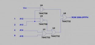
(The third column is the binary representation, and the second 0 from the left represents A14.) ROM is enabled whenever A14 is off, RAM enabled whenever it is on. With addressing circuitry this simple you'll see the following:
A: If you're using 8K parts each will appear twice inside each 16K window. IE, the contents of your 8K ROM will appear where you want them at location 0000, and then appear again at 2000. The reason for this is there's no decoding of A13 the 14th address line, the one that marks off 8K boundaries) and the chip only uses address lines up to A12 (13 of them.) The state of the lower 13 address lines counts up the same whether or not the 14th is on, the chip will be enabled for the whole time up until the 15th address line comes on, so it'll just spit out the same contents whether A13 is on or off. If you were to use even smaller parts you'd see even more repeated copies, IE, 4 copies for a 4k part, 8 copies for a 2k part. If instead you used a 16k part it'd fill the window perfectly. But:
B: There are four 16K windows in the address range, so each set (off/on) will also be repeated twice. (IE, the same memory that lives at the 0k mark will also appear at the 32k mark, and ditto the 16k and 48k windows.)
If you're stuck on 8k parts and having a gap between ROM and RAM bothers you decode A13 instead of A14 instead. Then RAM starts at 0x2000, right after ROM. But now you'll have a copy of ROM at the 16k mark, RAM at the 24k mark, ROM at the 32k mark... etc, etc, so it wastes the same amount of address space, just in a different pattern. Heck, if you really think that "8 kilobits" is the right number decode A10 to use a one kilobyte (
which is eight kilobits arranged into eight-bit bytes, as explained earlier) EPROM at 0x0000 and a one kilobyte SRAM at 0x0400. Then you'll have a copy of your entire memory map repeated every 2k boundary. If you don't want these shadow copies then you need to more fully decode the address spaces by adding more logic gates. And as BlackCow also noted you'll need to add some decoding hardware if you want to add any I/O chips to make this thing useful at all, unless just bit-banging the single I/O pin on the CPU is your idea of a good time.
And just for the record, no, I can tell you your test code is wrong even without knowing 8085 assembly simply because you're originating it at 0x4000. If you're mapping your EPROM at 0x0000 that's where you should ORG it in your assembler unless your design includes some sort of front panel, bootloader, or copy routine to load your test code into RAM and execute it from there. Someone else might be able to tell you if your delay loop is long enough to actually make the blinking of the LED visible to the human eye.
I think this was asked way back, but have you considered assembling a kit or playing with a well-documented microcontroller development board? Perhaps you could stand to work on your fundamentals a little more before building a machine like this from scratch.
")

")