• Please review our updated Terms and Rules here

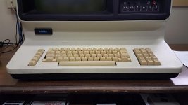
Lanier Model 103 "No Problem" word processor

As soon as I typed it, I thought about it. Been doing other things today.

That makes sense. Can certainly try to analyze what's what that way.

Also had a thought on the boot proms- I do have an Arduino board which could be used as memory and boot code provider.

Phil
 
I've found a couple test clips here. Should work, though I don't know the widest they'll go. I'll have a look.

The video display was stable when I drove the display to enable.

Reading the site where the other guy had his Lanier- he states that it beeps until you feed it a disc, and does nothing until then. I think potentially this one is halfway there; still unsure why it no longer pulls the disc drive head in though.

Agree that a Z80/8080 test set would be a useful device. Also if it had the capability to individually test 4116 style RAM.

--Phil
 
Agreed. I see there's some pull-up resistors on the video board, looks like the half-intensity background is triggered by that.

It's been a long time since I've dug into logic this deeply- when I did it last, it mostly focused on a bit of assembly and some basic troubleshooting. Really enjoyed it, but I'm having to change mental gear and try get back into the swing of it, beside everything else that's been happening here, family-wise.

EDIT: The chip clip is a 16-pin one and will fit neatly onto a RAM chip or otherwise single-width chip.

--Phil
 
Last edited:
U23 (7442)
1 => U56 #15
2 => U7 # 5
3 => U13 #4
4 => U13 #5
5-7 & 9-11 are n/c
12 => Tied low to ground
13 => U13 #2 & U22 # 5
14 => 8080 #38 & U52 #16 & U24 #15 ***
15 => U6 #3

U24 (7442)
1 => U5 #5
2 => U5 #3
3-7 & 9-11 are n/c
12 => U63 #3 & U11 #4 & Edge connector 24
13 => U38 #10 & U15 #3 & U3 #9
14 => U13 #1
15 => U23 #14 ***
 
So, the A B C on U23 are tied in to a few things, D held low. Outputs 0 thru 3 are used.

U24 had A B C and D tied in but only outputs 0 and 1 are actually connected.

Little confused as to why so few of the decode lines actually hook into anything.

I guess I need to dig the next layer down and see what the chips the outputs are hooked to and work forwards from there.

20150414_161529.jpg
http://oldbrokenjunk.com/gallery/var...g?m=1429056590

Today's trace-out.


--Phil
 
Last edited:
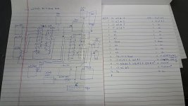
Probed out the board using the PROM as a starting point.

(Untidy, slightly inaccurate drawing removed).
http://www.oldbrokenjunk.com/gallery/var/albums/Lanier_103/20150415_103104.jpg?m=1429111920

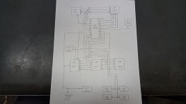
Links back to yesterday's diagram of U23 #1, the enable. Does lead out nicely to 4 of the DRAM chips, as you had surmised.

ERROR on the diagram there.. marked U39 is actually U43 and the DRAMs are labeled wrong.

I'm going to re-draw it.

**Edit- New diagram further down the page.

--Phil
 
Last edited:
Al,

No, not yet. I don't have anything to dump it with.

I hadn't seen that one on eBay- bit out of my price range, shame as it's not a horrendously far distance away (8 hours each way from here). Looks to be a slightly different variant based upon the case- probably the only difference. I need to Retr0bright the keys on this, it looks nice without the keys being yellow!

Would be nice if someone on here has picked it up.. I need a copy of those disks!


--Phil
 
Last edited:
Okay. I have a fair bit of work to do on it, but this weekend is filled with baking cakes with the kids and doing cake competition. Today is busy after work also, and my new boss is coming in to say hello today so probably not best to have my nose buried in a 9kV-exposed box not-technically-doing-my-job for today...

--Phil
 
I've discovered the Lanier boards do have a lot of chip-hidden traces. That and traces that jump sides, branch, jump back again.. all the usual culprits.

I can possibly work on the pinouts, working from key points (8080, RAM enable and data-in/out lines) to try and build a full schematic up. I'll see how things go. Shame I don't have a bed of nails but multimeter and paper will have to do. At least my meter beeps.

--Phil
 
Just in case, I've bought the CPU card's worth of 4116 RAM (18 chips). It's 150ns, the CPU card takes 300, the video card 350. As such, it'll be compatible with both.

--Phil
 
If the photos aren't clear enough I can try take some more, I have a slightly better camera now. That or I could put them on the flatbed scanner and see how well that works.

--Phil
 
Slight change of repair today.

20150422_172432.jpg

Took the heat gun to the fiberglass on the front and bent it (mostly) back into shape.

Needs cleaning more and the keys do look horrible in yellow.

Another thing for another day.

Phil
 
Last edited:
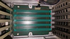
Solder side on all three is facing the screen.

It would appear there is an "aux" slot and one for a modem (which from the Super No Problem, would appear to be a twin RS-232 interface).

I'll check which one's which tomorrow and the order they are in. The backplane is marked.

Edit: Solder side of the backplane we have the following:

Code:
[FONT=Courier New]
           |           |           |           |  
  2     1  |  2     1  |  2     1  |  2     1  |  2     1
           |           |           |           | 
  s     c  |  s     c  |  s     c  |  s     c  |  s     c        (solder/component)
           |           |           |           |  
  100  99  |  100  99  |  100  99  |  100  99  |  100  99
-----------+-----------+-----------+-----------+-----------
   Option  |   Video   |    I/O    |    CPU    |   Comm.[/FONT]


Phil
 
Last edited:
Adding to your diagram... the backplane connector names from the solder-side photo.

Code:
+-----------+-----------+-----------+-----------+-----------+
|   Option  |   Video   |    I/O    |    CPU    |   Comm.   |
|    J1     |    J2     |    J3     |    J4     |    J5     |
|Notch: @30+|Notch: @36+|Notch: None|Notch: @40+|Notch: @30+|
+-----------+-----------+-----------+-----------+-----------+
|           |           |           |           |           |
|  2     1  |  2     1  |  2     1  |  2     1  |  2     1  |
|           |           |           |           |           |
|  s     c  |  s     c  |  s     c  |  s     c  |  s     c  |     (solder/component)
|           |           |           |           |           |
|  100  99  |  100  99  |  100  99  |  100  99  |  100  99  |
+-----------+-----------+-----------+-----------+-----------+


Tonight I'll add the connector pinout to the pin-list and maybe add a quick set for the discrete components. I might add the resistor pack pinouts too.

I'll email you attachments Friday or Saturday with:
1) Image: CPU Card Component-side Reference Designators with Corner Pin Numbers.
2) Image: CPU Card Solder-side Reference Designators with Corner Pin Numbers.
3) Text File: CPU Card Pin-List (for reference or quick lookup).
4) PDF File: CPU Card Pin-List color print of item 3.

Recommendation: Because ohming out the net connections of a printed circuit board is an exhaustive task, I'd recommend saving your time and patience until after the image net-list is taken as far as it can go. Because of hidden traces and hidden vias under chips, you'll have a lot to do in Phase 2. Best not to burn out early.

Usually I don't do a schematic palette of the chips until the net-list is complete, as its the first step of capturing the schematic from the list. But I think that a PDF of that schematic with parts only could be a useful document as you work with the CPU card diagnosing any problems with its bootup. I'll do that this weekend as it should be easy because I've already documented all the chip pinouts, names, and type in the spreadsheet lookup table.

By the way, the lookup table in the spreadsheet looks like:
Code:
Type	Desc	Pin-01	Pin-02	Pin-03	Pin-04	Pin-05
74'02a	NOR	1Y	1A	1B	2Y	2A
74'02b	14 Pin	o	'	'	o	'
74'04a	INV	1A	1Y	2A	2Y	3A
74'04b	14 Pin		o	'	o	'
74'08a	AND	1A	1B	1Y	2A	2B
74'08b	14 Pin	'	'	o	'	'
74'124a	VCO	2FC	1FC	1RNG	1CX1	1CX2
74'124b	16 Pin	'	'	'	'	'
There are two lines for every chip; makes it easier to align the pin type with the pin name. The table width allows for 40pins and 100 unique components for now. It just has the chips from the CPU card and a few I copied into it from the Exidy Sorcerer project.

The CPU card chips sorted by pin count ("(S)" for socketed) then chip type (the Lookup Names):
Code:
U07	14p	74'02	Quadruple 2-input positive NOR gates.
U05	14p	74'04	Hex inverters.
U27	14p	74'04	Hex inverters.
U34	14p	74'04	Hex inverters.
U13	14p	74'08	Quadruple 2-input positive AND gates.
U19	14p	74'125	Quadruple bus buffers with 3-state outputs.
U22	14p	74'20	Dual 4-input positive NAND gates.
U02	14p	74'32	Quadruple 2-input positive OR gates.
U06	14p	74'32	Quadruple 2-input positive OR gates.
U48	14p	74'32	Quadruple 2-input positive OR gates.
U60	14p	74'32	Quadruple 2-input positive OR gates.
U14	14p	74'38	Quadruple 2-input positive NAND buffers with Open-Collector outputs.
U03	14p	74'74	Dual D-type positive-edge triggered flip-flops with preset and clear.
U04	14p	74'74	Dual D-type positive-edge triggered flip-flops with preset and clear.
U15	14p	74'74	Dual D-type positive-edge triggered flip-flops with preset and clear.
U11	14p	DIP14	ResPak 220/330 ohms termination
U29	14p	DIP14	NOT POPULATED
U62	16p	74'124	Dual voltage controlled oscillators.
U16	16p	74'366	Hex inverter bus drivers with 3-state output.
U23	16p	74'42	4-line BCD to 10-line decimal decoders.
U24	16p	74'42	4-line BCD to 10-line decimal decoders.
U01	16p	DIP16	NOT POPULATED
U08	16p	DIP16	NOT POPULATED
U09	16p	DIP16	NOT POPULATED
U10	16p	DIP16	ResPak 2.2K ohms
U12	16p	DIP16	ResPak 2.2K ohms
U30	16p	DIP16	Switch 8 Bit Toggle Switch
U31	16p	DIP16	ResPak 2.2K ohms
U37	16p	DIP16	Switch 8 Bit Toggle Switch
U35	16p(S)	P8216	4-Bit parallel bidirectional bus driver.
U41	16p(S)	P8216	4-Bit parallel bidirectional bus driver.
U46	16p(S)	P8216	4-Bit parallel bidirectional bus driver.
U47	16p(S)	P8216	4-Bit parallel bidirectional bus driver.
U54	16p(S)	P8224	Clock generator and driver.
U17	16p(S)	PD416	Dram 16Kx1-bit.
U18	16p(S)	PD416	Dram 16Kx1-bit.
U25	16p(S)	PD416	Dram 16Kx1-bit.
U26	16p(S)	PD416	Dram 16Kx1-bit.
U32	16p(S)	PD416	Dram 16Kx1-bit.
U33	16p(S)	PD416	Dram 16Kx1-bit.
U39	16p(S)	PD416	Dram 16Kx1-bit.
U40	16p(S)	PD416	Dram 16Kx1-bit.
U44	16p(S)	PD416	Dram 16Kx1-bit.
U45	16p(S)	PD416	Dram 16Kx1-bit.
U50	16p(S)	PD416	Dram 16Kx1-bit.
U51	16p(S)	PD416	Dram 16Kx1-bit.
U57	16p(S)	PD416	Dram 16Kx1-bit.
U58	16p(S)	PD416	Dram 16Kx1-bit.
U64	16p(S)	PD416	Dram 16Kx1-bit.
U65	16p(S)	PD416	Dram 16Kx1-bit.
U55	20p	74'273	Octal D-type flip-flop with clear.
U38	20p	74'374	Octal D-type transparent latches and edge-triggered flip-flops.
U43	20p	74'374	Octal D-type transparent latches and edge-triggered flip-flops.
U52	20p	74'374	Octal D-type transparent latches and edge-triggered flip-flops.
U36	20p	81'95	Octal buffers with tri-state outputs.
U49	20p	81'95	Octal buffers with tri-state outputs.
U59	20p	81'95	Octal buffers with tri-state outputs.
U61	20p	81'95	Octal buffers with tri-state outputs.
U56	20p(S)	TBP1842	512 x 8 Prom.
U21	24p	P8212	8-bit output port and input port.
U20	24p(S)	P8214	Priority interrupt control unit.
U63	28p(S)	D3242	Memory interface integrated circuit.
U42	28p(S)	P8228	System Controller and Bus Driver
U28	40p	P8257	Programmable DMA controller.
U53	40p(S)	P8080	CPU microprocessor.
This ordering made quick work of the spreadsheet generated pin-list. I did all the 14 pin chips first, the 16 etc.

For each pin count type, I made/modified one chip pattern block that required only the chip type and the reference designator be entered. It used that to build the rest of the fields and to extract pin names and pin types and notes from the lookup table.

I'd block copy that pattern to the bottom of the pin-list for each reference designator. Repeated types were easier done at the same time because only the reference designator needed to be changed; hence this ordering.

When done I just sorted the first column of the pin-list to restore it to U01-U65 order and converted the entire pin-list block to values-only so it didn't have to recalculate or re-lookup anything.

This end result for chips only:
Code:
Empty	16 Pin	
DIP	U01	
	U01-01	
	U01-02	
	U01-03	
	U01-04	
	U01-05	
	U01-06	
	U01-07	
	U01-08	
	U01-09	
	U01-10	
	U01-11	
	U01-12	
	U01-13	
	U01-14	
	U01-15	
	U01-16	
		
74'32	14 Pin	
OR	U02	
1A	U02-01	
1B	U02-02	
1Y	U02-03	o
2A	U02-04	
2B	U02-05	
2Y	U02-06	o
GND	U02-07	g
3Y	U02-08	o
3A	U02-09	
3B	U02-10	
4Y	U02-11	o
4A	U02-12	
4B	U02-13	
VCC	U02-14	p

etc etc etc...
		
		
PD416	16 Pin	
16KDram	U65	
VBB	U65-01	p
DIN	U65-02	
WRITE#	U65-03	
RAS#	U65-04	
A0	U65-05	
A2	U65-06	
A1	U65-07	
VDD	U65-08	p
VCC	U65-09	p
A5	U65-10	
A4	U65-11	
A3	U65-12	
A6	U65-13	
DOUT	U65-14	o
CAS#	U65-15	
GND	U65-16	g
 
Last edited:
That email address is fine. Attachment max 8Mbytes.

20150423_122330.jpg

Bus connectors on this one do not have any blocking segments in any of the sockets. I'll run through the power and annotate the backplane solder-side image. Sorry that one's on its side.

--Phil
 
Last edited:
Pin connectors for power, top to bottom:

+5v
+5v
GND
n/c (though comes up at 1.85V when on, shall scope that to see if it's a clock signal or something)
GND
+12V
-12V

--Phil
 
The images for reference designators will be lower rez than the photos you supplied as its just for display when working on the board. I'll likely re-size it for 800x600 or 1024x768 screen size and reduce the color depth so they'll be small files. I'm guessing 1024x768 would be your pick for your nearby computer. If you have another preference, let me know.

I'm good with any size/resolution/color depth. The computer I'm using mostly has a 1920x1080 screen so is capable enough in that instance.

Thanks

-Phil
 
Back
Top