• Please review our updated Terms and Rules here

My project: The SeaOtter Essentials Prototyping Computer

The other thing to be concerned about with modern high current drivers not designed with controlled risetimes is they are fast
and if you aren't designing with transmission lines in mind they will ring like a bell.
Designers could be very sloppy with their busses in the LSTTL era.
 
Yes, but note those ICs sported an Iol of 24 ma, not the usual LSTTL 8 ma.

But the drive currents we're "concerned" about here are specifically the buffers in front of the 80188, all of which are *designed* to have good fan out. (IE, in the case of the original PC it was '373s and '244s, that's pretty much what we're dealing with on this design.)

Just scanning the schematics for the 5160 it looks like IBM was pretty conscientious about putting a second level of buffers after the CPU buffers where they felt like it'd be a good idea (for instance, they have additional '244s on A0-19 to create XA0-19 for most (but not *all*) of the onboard decoders and peripheral chips to reference, but they're still getting to, I dunno, looks like four or so LS loads before the signals even end up on the *eight* bus connectors. It's pretty *not* unusual for ISA cards to play a little fast and loose with buffering the ISA address lines privately, so you've got to figure that any XT that has more than a couple cards in it is fanning out to at least the ballpark of the number of loads the OP is considering with this project of theirs.

(I'm too lazy to count the fanout of the XA lines, but it's definitely also in the ballpark of 10+ devices. Also, FWIW, you have the MA* signals derived from plain old 74LS158s driving the memory sockets with a total fanout of 32; to accomplish this it looks like IBM slapped in some mild pull-ups.)

Anyway, yeah, it's not like we're building a Cray here.
 
Just scanning the schematics for the 5160 it looks like IBM was pretty conscientious about putting a second level of buffers after the CPU buffers where they felt like it'd be a good idea (for instance, they have additional '244s on A0-19 to create XA0-19 for most (but not *all*) of the onboard decoders and peripheral chips to reference
Block diagram of the address buses at [here].
 
The fan-out for LS logic outputs to LS inputs is usually good for around 20 or so, and if you really needed to stretch it you could strategically add some pull-up resistors.
Might that be why in the move from the IBM 5170 to the 5162, IBM added resistor networks to the SD bus ?
Crude diagrams at [here] and [here].
 
Might that be why in the move from the IBM 5170 to the 5162, IBM added resistor networks to the SD bus ?

Possibly, sure.

Anyway, I guess this whole thread kind of feels like someone looking at a few flower pots' worth of dirt and worrying they'll need a Caterpillar 797F to haul it across the yard. Pretty sure that a wheelbarrow will do. There's nothing earth shattering about the requirements here, it only looks "big" compared to the kind of five-chip Z80 SBCs that everyone and their dog are able to do today.
 
  • Like
Reactions: hmb
WARNING: Lots of text and images
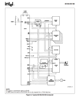
Hello. In my last post about my 80188 Computer project, called the SeaOtter Essentials Prototyping computer I talked about details of the computer itself. However, I wasn't happy about the Layout of all of the components on the PCB and the size of the PCB. It all felt a little too big. So I spent some time to create a smaller PCB with a neater and better component layout. The first board design only had 4 PCB layers, this new design has 8 PCB layers. Here are the results of my hard work and effort:
all PCB Layers (No GND Planes) + Length and Width MeasurementsTop PCB LayerInner1.pngInner2.pngInner3.pngInner4.pngInner5.pngInner6.pngBottom PCB Layer
Screenshot (144).png

I am very proud of the improved PCB design I've created. This design to me looks more organized and pleasing to look at. Now, as for my response to the post I've created before this one, I've decided to use 74HCT series logic chips because of their TTL compatibility and low current consumption. However, when I add a serial and an I/O Controller, I'll upgrade to either 74ABT or 74BCT because those logic chip series are designed for driving system busses and have a high current capability that's TTL compatible, which will be useful for when I need to add the Bus Transceiver ICs to separate the Data Bus from the multiplexed AD0-7 pins. I do apologize for not making my concerns over what Logic Chip series clear. I was mainly concerned with the fact that Address Line A0 is branched between the Keyboard Controller, VDP and an LCD Screen I'll use for debugging. I've found all of the Part I need from DigiKey and I'll leave a list below:
Now, All but one of these parts are labeled "SN74HCT___N", except for the 74HCT21, which as you readers can see has "CD" before the model number and "E" at the end. Does that mean I can't use the CD74HCT21E because its not a "SN74HCT___N" labeled chip, or does the "SN74HCT___N" and "CD74HCT___E" parts of the model number mean nothing and the only thing that matters is the fact that it's still a 74HCT series chip? (I'm sorry if this is an extremally stupid question to ask)

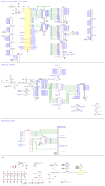
However, Before I'll order this new PCB, I'll need to test everything out on breadboards. I've made a 80188 breakout board in EasyEDA. I'll show the design in a reply to this post because Posts have a 10 image limit. Also in that reply, I'll show pictures of the hardware I've collected for this project.

As always, Thank you guys for reading and if any of you guys have any advice for me, It'll be thanked in advance!
 
Well, the SN is the manufacturer (Texas Instruments) in general.

Manufacturers do not waste space in adding alphanumerical data to part numbers. In general, every location means something. Check the data sheets for the parts. They may be something inconsequential as the temperature range; but it can also indicate something important such as the device packaging. It would be a shame to have designed a PCB using DIL parts only to find out that the component is something else!

Dave
 
However, when I add a serial and an I/O Controller, I'll upgrade to either 74ABT or 74BCT because those logic chip series are designed for driving system busses and have a high current capability that's TTL compatible, which will be useful for when I need to add the Bus Transceiver ICs to separate the Data Bus from the multiplexed AD0-7 pins. I do apologize for not making my concerns over what Logic Chip series clear. I was mainly concerned with the fact that Address Line A0 is branched between the Keyboard Controller, VDP and an LCD Screen I'll use for debugging

Sigh. The datasheet for the 74HCT245 clearly says it has drive capability for *15* LSTTL loads, as do the latches you’re using. Frankly this is coming across as paranoid.

If you’re really worried about signal integrity this badly why on earth are you running the CPU’s AD0-7 lines directly to everything instead of buffering them with a ‘245, like every other 80x88 computer on the planet does? That seems like a far worse design decision than not using Schwarzenegger-strength bus drivers for your completely unremarkable-scale-complexity small computer. Did you even look at the schematics for a similar system and count loads?
 
The first two letters are manufacturer-specific; for example, Fujitsu = MB, NSC = DM, etc. However, even this can only indicate the original part--stuff gets sold, so you can find TI using NSC's LM part numbers.

I recommend that you put the DIPs in sockets. That way, you can easily experiment with different logic families. I used the ABT transceivers because I was driving long (10' cables) terminated in 220/330. OC/OD in many part families is getting to be hard to find, but tristate does work in a pinch.
 
For 74 series chips the following applies

1692461586587.png

The CD prefix was traditionally Harris but they were acquired by Texas some time ago. The E suffix on a CD part is the same as an N on a SN part. Different manufacturers may have slight differences in the performance which you can find by comparing datasheets, in most cases it won't be a problem.
 
I used the ABT transceivers because I was driving long (10' cables) terminated in 220/330.

Sure. If the OP was planning to drive a 20 slot card cage several U removed from the system unit in a full height rack I would vibe with that recommendation, but this is just silly. This computer even with the proposed additions still has fewer parts than an IBM PC or Tandy 1000 has on the motherboard alone.

And I’m serious about my previous comment: unless I’m missing something it looks like the schematic for this computer has the raw AD0-7 (simply renamed “D0-7”) lines from the CPU not just running to every peripheral/memory chip on the main board, but terminating on a pin connector next to the latched A0-19 pins. Where is this huge concern for drive strength from the *naked CPU*, which at this point has at least, what, six loads on it before getting to the connector? This is hard to take seriously.

One look at the schematics for an IBM PC or Tandy 1000 will give the OP the standard template for building an x86 computer with a decent handful of onboard components and enough drive strength to run a good number (half a dozen at least) slots: Put the CPU behind ‘373/573’s to latch the addresses, bidirectionally buffer the data lines with a ‘245 or back-to-back ‘244s, (and also buffer the needful control signals), and then run all that crap to your slot connectors. Then add *another* ’245 for data and a set of ‘244’s on the address lines to ”reset” your fan-out and run *all* the onboard support chips/peripherals on that bus. (IE, this essentially makes all the onboard stuff a “peer” on the primary bus segment with the buffered CPU and the slots.)…

But that said, this design *isn’t* (currently) a “box of slots”, it’s more like a TRS-80 or VIC-20 or TI 99/44A, IE, a “small computer” with a handful of onboard peripherals and an unbuffered bus connector intended to handle daisy chaining a couple things off it. For that later situation, honestly, skipping dual layers of buffering for the onboard stuff is probably fine, if you really had to go nuts expanding it you could always buffer the bus externally to reset fan out. So from *that* standpoint the design is probably ‘fine’ as it is, at least as a prototype... but yeah, all this paranoia about address bus drive strength when there is *no* buffering at all on the data bus is just ridiculous.
 
this new design has 8 PCB layers. Here are the results of my hard work and effort:​

I am very proud of the improved PCB design I've created.

Oy. An 8-layer board is certainly not necessary for such a simple design (less than 20 ICs), and will cost at least 50% more than a 4-layer board that is 50% larger in both directions.

There are so many things that look like jokes here, but I'm not laughing. At this point I need to be convinced that you are not a troll.
 
I'd be very surprised if this couldn't be done with a 2-layer board. In any case, I'd probably use a NEC µPD70208H for the job--you can get them up to 20MHz--a lot friendlier CPU design. The D70216 16-bit seems to be plentiful also.
 
Last edited:
Sigh. The datasheet for the 74HCT245 clearly says it has drive capability for *15* LSTTL loads, as do the latches you’re using. Frankly this is coming across as paranoid.

If you’re really worried about signal integrity this badly why on earth are you running the CPU’s AD0-7 lines directly to everything instead of buffering them with a ‘245, like every other 80x88 computer on the planet does? That seems like a far worse design decision than not using Schwarzenegger-strength bus drivers for your completely unremarkable-scale-complexity small computer. Did you even look at the schematics for a similar system and count loads?
I was told that for a small 80188 computer, I don't need to use the bus transceivers for the Data Bus. The datasheet for the CPU shows a typical computer setup diagram of which I'll show in this reply.

It's this setup is what I'm using. I'll also add the schematic for this project as well.
 

Attachments

  • Screenshot_20230224-114354.png
    Screenshot_20230224-114354.png
    244.8 KB · Views: 6
  • Schematic_SO 8-Bit Essentials Prototyping Computer_2023-07-11.png
    Schematic_SO 8-Bit Essentials Prototyping Computer_2023-07-11.png
    1.3 MB · Views: 6
Oy. An 8-layer board is certainly not necessary for such a simple design (less than 20 ICs), and will cost at least 50% more than a 4-layer board that is 50% larger in both directions.

There are so many things that look like jokes here, but I'm not laughing. At this point I need to be convinced that you are not a troll.
I'm simply new to PCB designing. It's a hobby I've recently got into and I have a small amount of practice with the skill.

I apologize for the seemingly low effort quality I've put on display here.
 
Back
Top