T-Squared
Veteran Member
It's been a while, but I decided to take a serious look at this. (Since I have no other real projects on my plate at the moment, and I'm resting from getting back from a trip)Again, it's instructive to compare this to the 5150. If we trace that same RAMADDRSEL line on the 1984 schematics (64/256k system board) for the 5150 to sheet 3 of its schematic you'll see it terminates on U48, a 74LS138, that only has input lines connected to A18 and A19 so, again, its only choice is to enable the buffer when the board is in the bottom 256k of the address space. Likewise if you look at the inputs for U47 and U65 they're connected straight to A16 and A17 so there's no choice: each CAS/RAS pair covers a 64k area, no other options.
Now it's up to you to figure out if the Sanyo is *actually* hardwired as tight as the 5150. Follow the CAS/RAS lines back to where they come from (presumably also '138s) and figure out what their inputs are connected to. If they're straight through to A16 and A17 then it's hardwired for 64k no matter what A8 on the memory sockets does. If they are *not* then trace them back and find out if it's a PROM, a PAL, a bunch of random circuitry, *whatever*, that's connected to A16-A19 and has some kind of input for switching modes.
Just spitballing here, if this was a 5150 and you asked me to a way to hack it to 640k (and don't care about butchering it) I'd say try pulling the A/B pins on U47 and U65 out of their sockets, removing U48 entirely, running a few jumper wires, and programming a GAL with the following inputs:
A16-A19
ADDRSEL
DACK0BRD
These outputs:
MA8 (need to get this to pin1 on the DRAMs somehow, probably involves trace cuts)
CASRASDRVA and B (goes to A/B on U47 and U65)
RAMADDRSEL
And the appropriate memory map equations. "deadbug" the GAL somewhere, and, well, cross your fingers.
I have a suspicion the fix for the Sanyo will be about that extensive, but maybe they went the full mile building a full dual-mode decoder they never intended to use.
Someone was nice enough to send photos of their Sanyo MBC-675 motherboard, and it's completely different, so it's not much help to me.
Again, you need to start checking out the RAS/CAS generation and see if *its* inputs are connected straight to the address bus or if there's some kind of abstraction. If the inputs are direct from a '244 or '373 then it's almost a 100% certainty that the RAM bank addressing is hardwired for 64k chips *only*.
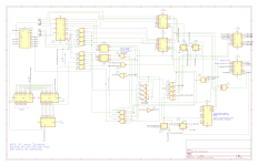
I rechecked my schematic, and RAS/CAS is not directly connected to a 244/373, and I found a discrepancy I forgot to add involving the Select + Strobe pins.
CAS/RAS 3 & 4 lead to a 157's outputs.
I thought that particular 157's Select pin (Pin 1) was not connected to anything, but doing some continuity, it's strangely connected through a 4.7kohm resistor directly to VCC! (To me, that doesn't make sense, unless it's supposed to be held high.) Also, there's a previously blank footprint for a resistor connected to the enable/strobe pin (pin 15), which I'm assuming is 4.7kohms as well, given that there are 3 resistors in the area (including one of those that is connected to the select pin).
I'm not sure if this means anything.
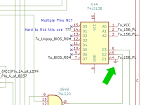
BTW, here's the area in-question on my schematic:

Last edited: