• Please review our updated Terms and Rules here

Original-IBM-5150 or IBM-Clone Memory Experimentation Thread

Sorry about the delay. Looking over my pin-routing, The RAS and CAS are fed to the memory ICs by a 157, a LS08 (AND gate), and a 138.

I'd have to check whether that matches up with any schematic I've looked over before. (If this feeds through the same types of logic gates present in those ICs)
 
Are you actually writing down a schematic for your machine as you're doing this? Because you really need a complete schematic to determine under what circumstances (IE, state of the address lines) which RAS/CAS pair is active. (And also for what address ranges that '245 on the RAM data lines is enabled.) Open up the 5150 and 5160 service manuals and look at sheet 3 of the schematics for both of those machines: What you need to know is what is *immediately upstream* of the '138s. (There should be two, one that directly supplies the CAS lines and the other that supplies RAS through the '08.) The input and enable lines (1,2,3 and 4,5,6) will connect to some combination of address lines and an address decoder. That address decoder is what you need to understand. Full stop. There are many things it could be, the 5150's schematic is the "simple" version and the 5160's is a fully programmable one. Diagram everything, accurately. There is no particular reason the Sanyo's address decoder should match either IBM machine's particularly closely, there are *many* ways this to skin this cat and you need to understand what Sanyo actually did.
 
Are you actually writing down a schematic for your machine as you're doing this? Because you really need a complete schematic to determine under what circumstances (IE, state of the address lines) which RAS/CAS pair is active. (And also for what address ranges that '245 on the RAM data lines is enabled.)

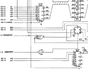
Not a schematic (yet), just a routing from a pin-listing of one chip to the other, with their corresponding silkscreen numbers (the 8088 and 8087 are off on the right) Sorry I can't make it any clearer:

Click image for larger version  Name:	Sanyo Pin Routing small.png Views:	0 Size:	227.8 KB ID:	1209401
Open up the 5150 and 5160 service manuals and look at sheet 3 of the schematics for both of those machines: What you need to know is what is *immediately upstream* of the '138s. (There should be two, one that directly supplies the CAS lines and the other that supplies RAS through the '08.) The input and enable lines (1,2,3 and 4,5,6) will connect to some combination of address lines and an address decoder. That address decoder is what you need to understand. Full stop. There are many things it could be, the 5150's schematic is the "simple" version and the 5160's is a fully programmable one. Diagram everything, accurately. There is no particular reason the Sanyo's address decoder should match either IBM machine's particularly closely, there are *many* ways this to skin this cat and you need to understand what Sanyo actually did.

And yes, I've already realized that what Sanyo has done doesn't match up perfectly in any way in places (i.e. It's mostly the same gates and same routing, but instead you're routing an input through the same gate in a different logic chip).
 
You know, I may have accidentally stumbled upon a reason for my Sanyo system not working with my memory chips...

Would bad memory in any form stop an IBM/clone computer from starting? It seems like I have a bad batch, according to what I have while testing my 41256 chips with my Macintosh 128k. (The memory tester I bought shows everything is fine, though, but I think even that can have false positives.)

When I started working on this project, there was a spot for a 139 IC. I think it was a multiplexer. The Macintosh 128k that I have also had an expansion footprint for a socketed/soldered 153 multiplexer.
 
Last edited:
I may have made some progress, and not needed to route anything!

I decided, on a hunch, to take out the parity generator chip, and test the system with the 640k, with the Supersoft Diagnostics.

It immediately started up, and all the memory tests I saw passed.

Later, I will be trying the system with the original ROM (The Yangtech Phoenix Turbo XT BIOS I use), and the EGA card that I have.


EDIT:

Well, the good news is, I seem to have solved the problem of the computer not even showing a picture or the CPU starting to execute code. The system now turns on with no problem. The bad news? The new memory is not being detected. I did test the 64k chips beforehand to make sure they were working.
 
Last edited:
I think the computer is detecting the 256kbit chips as 64kbit, because I only have 512 kilobytes of 256kbit memory, and 128 kilobytes of 64kbit memory (640 kilobytes total), yet the POST still counts 256 kilobytes of memory. (which doesn't match with either memory groups)

I wonder if the connection that's missing is simpler than we both think.
 
Looking back at the previous posts, I think the board and the 256k memory works, but Pin 1/Address 8 is not connected properly, because enough of the connections are there to make the computer work with the 512k/128k combined memory.

I will look at the board and trace A8 around to see if I need to jumper a connection with a wire.
 
I've traced the A8 pin back to a delay line, which I did before. Everything seems to match up so far. However, I noticed something on the board that I don't think was made by me: a small missable gouge that completely severed the connection between the delay line chip and the 139 chip that it's normally connected to.

The reason why I don't think I made that gouge is because the bodge wire connecting it does not exist on the extra MBC-775 processor board that I have, and the relevant trace is intact. Also, the wire was black, and it fit neatly between the connecting pins. (I'm good at that, but I normally overestimate the length of wires when needing to jumper points, so mine are longer and less clean-looking.) Finally, it's in-between the delay line and the chip, so it would probably be very difficult for me to do the damage that I found in that small of a space, and it's a relatively deep gouge. (approx .2mm)
The worst I've gouged a board is only enough to take off the solder mask.
I wonder if a small accident at the factory damaged it, and they put that bodge wire there to make it work again, so they wouldn't have to reject stock.

I didn't get any other change when I tried to move the wire to a delay timing closer to what the original 5160 has.

If the memory is being accepted, being read at startup, and the computer works just fine even though it's not seeing the other 384kb of memory, does that mean that the select line (the pin 1 A/B line on the memory) is not being toggled?
 
Last edited:
Okay, looking at everything else, the lines and logic seem connected. (I didn't have to re-map everything.)

From this point forward, everything now seems connected to the 244 and 373 logic equivalent of that 24S10 PROM used in the 5160, because the connections from A16-A19 on the CPU side, and the connections from A8 on the memory side all meet up there. Strangely, the connection to the 24S10-equivalent logic also seems to go off of the CPU/MEM board and onto the video/ISA/Disk controller board; apparently they didn't have enough room for the extra logic chips.
 
I meant to say that everything to solve now seems to involve the logic that normally is occupied by the 24S10 PROM. Maybe there's a connection missing there.
 
From this point forward, everything now seems connected to the 244 and 373 logic equivalent of that 24S10 PROM used in the 5160, because the connections from A16-A19 on the CPU side, and the connections from A8 on the memory side all meet up there. Strangely, the connection to the 24S10-equivalent logic also seems to go off of the CPU/MEM board and onto the video/ISA/Disk controller board; apparently they didn't have enough room for the extra logic chips.

The task of the 24S10 PROM in the 5160 is to act as a really primitive form of programmable logic. (Grandpa's first FPGA, har har.) A PROM is of course just a ROM; there are address lines going in and data lines going out. A given combination of address lines being on and off connects the data lines to an individual cell of memory inside the chip and the contents of that cell are expressed on the data lines as high and low states. Normally of course you'd have those data lines connected to the memory bus of a CPU or whatever, but a really common hack back in the day was to instead use the PROM data outputs as, say, chip enable signals, and then program the ROM data to emulate the behavior of the combinational logic you're subbing the PROM for. (I guess I already explained this on page 3.) As I said in that post, if your Sanyo doesn't have a PROM in it then you *need* to understand what it's using instead. Remember, again, the '244s and '373s have nothing to do with address decoding. Zero. They're just plumbing. An address decoder, if it's not a PROM, is going to include parts like '138 or '139s, maybe some AND gates (with variable number of inputs), etc. Or it could be a PAL, although I think this Sanyo might just be a hair to old for that.

In this post I outlined how comparing the 5150 schematics to the 5160's might be instructive because the 5150 uses combinational logic instead of the 5160's PROM. It's completely possible the Sanyo implemented a combinational logic decoder that still supports both 256k and 640k configurations, it's not that much rocket science, but if that logic requires a physical jumper to be soldered somewhere or other physical change instead being "soft-switchable" then you're going to have to figure that out to get it to "see" the memory you added. Or it's possible Sanyo only partially implemented the 640k capability (IE, the traces/etc for the A8 multiplexing were on the PCB, but actually using them requires some component substitution in the decoding section.) Have you drawn out the decoding? From your vague description it sounds like you might just be getting the enable lines for RAM via a decoder that lives on another board? That's actually not that crazy for a machine with "built-in" peripherals like this; RAM is just another peripheral so it may well share a discrete logic decoder that also supplies enable lines for, say, the CGA memory.
 
All I know is that when I replaced the memory, it started to work Previously I had errors like you see in the video.

Ignore most of the captions, and yes, I know the Supersoft Diags are not baseline diags, but these errors were consistent until I replaced the memory, so I don't know what's going on...:

Also, I was wrong, at least one line for the higher addresses does lead to a 138, so there's still a chance. (I've had 244s and 373s staring me in the face so long that they've lodged into my mind.)
 
Last edited:
Question: Since the memory is working even though the extra capacity is not being read, that means the address lines are working properly, correct?

So that means that the A8 line is the focus of this mod, and responsible for addressing the extra capacity in the 256kbit chips, correct?
 
Will an IBM 51X0 system count up only to the amount of RAM that it is able to address?

To clarify, if one address line was severed or not connected, would that drop the amount of memory detectable by the system (like the cheap 16kbit memory, which was actually faulty 32kbit, but still worked) that Sinclair used in the 1980s, or would that break the system entirely? This is assuming that there's some kind of POST failsafe in the BIOS that drops the amount of addressable memory to a power-of-2 or divisible amount and ignores the faulty RAM beyond that point. (i.e. 512kbyte of RAM, but 128k is not properly addressable [maybe 16k does not work], so it drops to 384kbytes.) Of course, I may just be spitting smoke.

I seem to have found an address line (A17) that may not be connected to anything, and may be my problem. (It's not connected to any 37x, 24x, or 138 logic chips.) I'm not sure yet, though. I'll have to continue probing with the multimeter in order to find out.
 
Will an IBM 51X0 system count up only to the amount of RAM that it is able to address?

IBM 5150

The POST displays no RAM 'count-up'.
The POST is informed of the total amount of conventional memory (motherboard + cards) is fitted in the computer by way of switches on the motherboard.
The POST will test that amount.

IBM 5160

Flawed methodology.
See the 'Flawed methodology for determining total conventional memory size' section of [here].

(Related information at [here].)

IBM 5162 and IBM 5170

The POST is informed of the total amount of conventional (base) memory is fitted in the computer by way of a figure stored in the CMOS SETUP.
The POST is informed of the total amount of extended (expansion) memory is fitted in the computer by way of a figure stored in the CMOS SETUP.
The POST will test those amounts.
 
I skimmed over that about that a few days ago, but didn't think much of it. It does seem to match my idea. (At the very least, A8 seems to not be activating properly.)
 
Will an IBM 51X0 system count up only to the amount of RAM that it is able to address?

To clarify, if one address line was severed or not connected, would that drop the amount of memory detectable by the system (like the cheap 16kbit memory, which was actually faulty 32kbit, but still worked) that Sinclair used in the 1980s, or would that break the system entirely? This is assuming that there's some kind of POST failsafe in the BIOS that drops the amount of addressable memory to a power-of-2 or divisible amount and ignores the faulty RAM beyond that point. (i.e. 512kbyte of RAM, but 128k is not properly addressable [maybe 16k does not work], so it drops to 384kbytes.) Of course, I may just be spitting smoke.

Long and short of it is no, not unless the computer is equipped for such a situation in hardware. I'll try to explain momentarily.

I seem to have found an address line (A17) that may not be connected to anything, and may be my problem. (It's not connected to any 37x, 24x, or 138 logic chips.) I'm not sure yet, though. I'll have to continue probing with the multimeter in order to find out.

Maybe it's part of your problem, but it's not your whole problem. But let's start here:

address_multiplexer.png
As laboriously gone over earlier, U84 on this snippet from the IBM 5160 motherboard schematic is one of the (important) differences between this board, which supports 256kbit RAMs, and the (later version of) the 5150, which only supported 64kbit. Again, rehashing what we already know, it's a multiplexer with two used inputs, XA16 and XA17, buffered versions of the CPU's A16 and A17, and the output derived from them is MA8, which is connected to pin one of all the memory sockets. The input "ADDRSEL" is used to switch which input appears on the output depending on which part of the RAS/CAS cycle we're on. Two address lines is two bits, the number of possible combinations in two bits is four, so if everything is working right the addition of this part is what lets the same sockets hold four times as much memory; a line that's unused on 4164 chips turns into (effectively) two additional address bits. This means, tada, the same array covers 18 address bits (2^18, 256K, instead of 2^16, 64k).

So... obviously, this is a problem if A17 isn't connected to this multiplexer; it means that either RAS or CAS will always present the same value to A8, and this reduces the total size of the memory bank to 128k. If the memory *addressing circuitry* were set up to expect 256k in a bank this isn't a "self-healing" problem, one half of the 256k range of that bank will just address a duplicate of the other because of the stuck bit. In some hypothetical situation where you were sitting on a pile of 41256s that you knew all had the same half of the chip "bad", sure, you could take advantage of this by going ahead and populating those chips into banks and setting up the address circuitry accordingly. (Per your reference, they actually did this with half-bad 16K 4116 chips back in the late 1970's; they sold them as "4108s" and they were used in Commodore PETs, among other things.) But I absolutely 100% don't think this is what's happening in your Sanyo. Full stop.

If you have a logic probe or oscilloscope I would by all means suggest you probe the "XA16" and "XA17" inputs on the '158 multiplexer you added to control A8 to see if they're changing; if you see XA16 pulsing and XA17 not pulsing then you know, full stop, that the 256K banks will not work, and that's useful information, but whether they're pulsing or not I'm am positive that it doesn't matter, your memory decoder isn't set up to make use of the full capacity of these banks. Even if everything is working here I think you're only set up to use a quarter of the capacity of the 256K banks, the only thing having this circuitry working is going to change is which quarter you're using in each bank.

Here's another screenshot from the 5160 schematic. Completely forget about the memory array right now, full stop, other than this: Each row of sockets are all wired in parallel except the CAS/RAS lines. It is the CAS/RAS line activity that triggers read/write/refresh cycles on the chip:

Screen Shot 2022-01-28 at 10.31.38 AM.png

See how A16-A19 feed into that 24S10 chip (and some lines that go to DIP switches and jumpers, but we're ignoring those right now), and three control lines come out. The 24S10 PROM programmed with a bitmap of information so for a given memory address (with 64K granularity, because it only sees the top four address lines, letting it break the full 1MB of address space into 16 chunks) it activates some combination of output lines. The first, "RAMADDRSEL", comes on if ANY memory on the planar is supposed to be active; it controls the buffer in front of the memory chips which asserts control of the bus if it thinks the memory chips should be answering the bus request. The other two lines coming out of it are a two bit bank select. Based on the memory address one of four bank numbers 0 through 3 will come out of these lines. It is the programming of this PROM that "knows" if a bank is supposed to have 256k or 64k in it, and what areas of the memory map that bank is going to cover.

The bank output from PROM goes to that pair of LS138s labeled U42 and U56, which decode the "multiplexed" binary number into a singleton CAS0-3 or RAS0-3 signal. They're 1-of-8 selectors (of which half of each is being wasted, turning them into 1-of-4 selectors) so only one memory bank will get an active CAS/RAS at a time. Thus... and there's the part I keep repeating: It doesn't matter if you fixed up the memory bank so it's "256K big" instead of "64K big" if this part of your Sanyo doesn't know about it. As it came from the factory your Sanyo was set up so it broke the first 256K of the 1MB address space into four 64K chunks, and activated a separate CAS/RAS pair for each of those chunks. If you haven't adjusted that and just substituted 256K chips in the bottom two banks, again, even if everything is working perfectly in that area here is what your memory map is going to work out as at a hardware level:

0-64K: provided by the first 64k of the 41256s in bank0. (A8 will be zero on both CAS and RAS)
64k-128K: provided by the second 64K of the 41256s in bank1 (A8 one on RAS, zero on CAS)
128k-192k: provided by the 4164s in bank2. (A8 zero on RAS, one on CAS, the 4164s don't care about A8, return the same 64k regardless)
192k-256k: provided by the 4164s in bank3. (A8 one on CAS and RAS)

Unless I missed the part where you redid this part of the circuitry all the fooling around in the world with the memory banks themselves isn't going to change when they're enabled. Now, sure, in some later computers the computer can figure out itself what size memory chips are installed in a bank and switch to a memory addressing scheme that suits it, but I absolutely guaruntee your Sanyo doesn't have that implemented. (The 5160 doesn't either; it can guess if a bank is populated but it can't change its addressing behavior if you stick the wrong size into a bank.)
 
Okay, the logic probe seems to show A8 being constantly pulled low, but XA16 and XA17 are pulsing.

(Just to make sure, also I checked one of the other address lines. It's pulsing too, and the computer works just fine, so it's probably a good assumption that the rest of them are working properly)

What does that point out?
 
Last edited:
Oops. I was reading the wrong pin. Pin 1 (A8) is indeed receiving the pulses. The A16 and A17 lines that operate the 158, as well as the 158 itself, seem to be in working order. We can ignore the 24S10 PROM altogether.


So... I'm guessing now we move onto RAS and CAS?
 
Last edited:
Back
Top