• Please review our updated Terms and Rules here

PC 5170 need help with PAL16L8 and 28S42

That's an annoying thing about the blog section--there is apparently no way for one to remove entries made in error--mostly by clicking the "blog this post" instead of the "reply to thread" right below it. I don't really understand why the "blog this post" button is there to begin with.
 
Last edited:
Nice but what about 3state outputs?
Dwight

I address this in the later parts of the blog. I employ a little trick to gently "push" on outputs to determine if they're tristate. If I gave more thought to this in retrospect, I could have worked the "push" logic with just a single output. In other words, run the exhaustive test of combinations with and without the "push" and compare the results.

However, I've had no need to clone PALs in quite a few years, so this has dropped off the radar for me.

I guess I got tired of pushing next. Most applications don't use the 3state anyway. They are usually just address decoders.
Dwight
 
So nobody has made copies of the PAL's on the 5170? I'd sure like copies to burn if they have so I can have them on hand if needed. Best I can tell there are 3 of these on the 5170 type 1 board.
 
I also ran U130 through LF and got the same minimizations.

Code:
IRQ13 = ERRORn' ;
BUSY286n = 0;
NPCSn = XA3' + INTAn'  + CS287n  + SMIO ;
RESET287 = INTAn CS287n' SMIO' XIOWn' XA0 XA3' + RESET ;

Every book i read on this topic says that the BUSY Pin of the 287 coprocessor should be connected to the BUSY Ping on 286. I checked the schematics and your guys' Truth table and it seems that,
1. The BUSY Pin on 286 is always 0 which would mean: always active
2. The BUSY Output signal of 287 would not be routed to anything except input to U130 and as such it would be useless.

Can anybody help me understand this part of PC AT schematics?
Thanks
 
Hello everyone,

I know this thread has been inactive for a while, I came across it in a search for how to get the logic from PAL16L8 ICs, specifically U87 and U130 in the IBM 5170.
I'm doing a project to design my own recreation of an 5170-alike PC mainboard. The thread can be found here for anyone interested.

First of all my thanks to newold86 and eeguru for the work you have done and shared here so far. There is no useful definitive information about U87 and U130 to be found anywhere as far as I know, so your information is at least the closest source to be found at the moment. Which is why I posted here in the hope that the definitive versions could be finally known to those who seek this information and come across this thread.

As the thread concluded so far up to now there was the issue remaining that the equations assembled so far were not complete.

This will be due to the complexity of the PAL programming as done by IBM originally, which may make finding the original logic more difficult than the straight evaluation methods we can find from various sources. There is some mention of this problem on various websites pointing this out that in certain types of PAL programming there may occur some fast flipping of outputs which trigger internal changes in the logic states for example.

At first I had some high hopes that reading a PAL as an EPROM with some additional resistors could yield the logic, however right now after doing further reading on the subject I am not entirely hopeful that this may lead to the complete logic as programmed originally. Though there may still be some partial clues to the logic that can be concluded from the equations shared in this thread. I did not crosscheck these equations in this thread yet with my own work and research, which I probably should do before my project proceeds to further stages, I plan to.

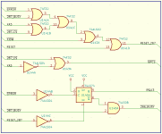
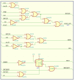
I have studied a few sources of information and first found some clues about U130, from a functional perspective to find descriptions of what is expected to happen inside U130, which can be somewhat deduced I believe by what I found. So far I got some information from the VLSI datasheet of the VL81C101B AT chipset IC and from some schematic photos of the Copam PC-501 Turbo PC. Combining all the information so far, I was able to compose an approximation of the logic.

A few cautions, using this info is at the sole risk of the user, there are no guarantees if this will even work at all, maybe it doesn't. Only attempt to use it for anything if you are experienced in doing this type of work and accept the risk of breaking stuff in the process. That's a general comment I want to state here. I will be testing this and other solutions in the interest of my ongoing project.

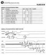
The VLSI datasheet has documented some useful timing constraints which may be relevant in the circuits and logic IC families that could possibly provide a functional coprocessor/CPU control method, which is what U130 is involved in. I will be testing my best effort version after doing a lot more research and checking against the PAL IC itself to see if the logic is indeed behaving in a similar way. I will probably wire up some switches and LED outputs to be able to see what happens if I assume the logic to be what I share here. Not that this setup can reveal all possible problems but at least it may give me some more confidence.

I have attached a useful page from the VLSI datasheet showing the timing of the /ERROR condition when it occurs, and is cleared by a 287_RESET being asserted.
The other attachment shows what the circuits might possibly look like.

The logic types are not conclusive and neither are the gates used, this is just a first attempt to at least compile things in some circuits for starters.
For example the RESET action on the 74LS74 may need additional logic for synchronization or timing delays, which also applies to other areas.
I saw some numbers of 35ns in the VLSI datasheet which seems long and definately in some areas the preference may be to use LS or other slower logic.
So some experimentation may be needed to get it right, such as swapping gates or adding more gates in between, even if the logic is functionally correct.

Needless to say, I will be pushing on in my project which has a huge amount of work to be done.
I will post more in the future in the previously mentioned thread of my project, and PAL related stuff I can share here in this one if anyone is interested.
As mentioned before, it's puzzling that this PAL info is not yet known, and I believe such a brilliant design by IBM really deserves to be preserved, the way I see that to be possible is at least to document the technology completely which my project will certainly attempt to do in my own way.

This is what I have so far, I am sharing everything I find with the community and my 80286 PC project based on the 5170 concept will be published on GitHub as soon as it is completed.

I believe in sharing knowledge and pooling efforts together which is to me the best way that great things can be achieved by us.
If anyone has some comment or useful info please share it here, I would appreciate any and all help!

Kind regards,

Rodney
 

Attachments

  • U130_version_001.png
    U130_version_001.png
    14.8 KB · Views: 8
  • 000 CPU - NPU interaction timing diagram with error condition VTI_ComputerProducts_1989.pdf
    40.7 KB · Views: 7
Here is a copy of my notes about U130 so far:

Code:
/BUSY_287
a busy status input that is asserted by the 80287 to indicate that it is currently executing a command.
0 = coprocessor busy
1 = coprocessor inactive


/BUSY_286
Processor 286 extension busy - this signal goes to the /BUSY input of the CPU.
If pulled low, this signal stops the CPU execution on all WAIT and some ESC instructions
until it returns inactive high again
0 = stop CPU
1 = CPU continue


/NPCS  
coprocessor chip select active low
decoded at I/O on port 0F8-0FF
98    7654    3210
00    1111    1xxx
/287_CS


RESET287
active high signal to reset the coprocessor
activated by
- a system reset
- I/O write to 0F1 or 0F1


/ERROR
an error status input from the coprocessor
this reflects the ES bit of the coprocessor status word and indicates that an
unmasked error condition exists


The coprocessor asserts /BUSY_287 when it is executing a task.
This is passed through to the CPU on input /BUSY_286
Normally /BUSY_286 will follow /BUSY_287,
however if /ERROR is asserted while /BUSY_287 is active,
the /BUSY_286 output will be latched low and remains low,
until it is cleared by an IO write cycle tco 0F0 or 0F1.
/IOW and 0F0 or 0F1 asserts a RESET287.
condition for this assertion of RESET287:
/IOW is low
XA5-9 -> /287_CS asserted low at 98765 = 00111 and /ACK inactive high
XA3
XA0
set accordingly
98    7654
00    111x    0Ex    /287_CS is 0
00    111x    0Fx     /287_CS is 0
full condition looking at PAL inputs and PDF by VLSI:
98    7654    3210
00    111x    000x    0F0 or 0F1


decoder with inputs:
- RESET        if 1, directly assert RESET_287 high
second condition from:
- /287_CS    0
- XA3        0
- /XIOW        0  
- /ERROR    0
- /BUSY_287    0
output:
RESET_287

If I made any error or something is missing here, anyone feel free to comment, thanks.

I converted the VLSI PDF page to a bitmap, sorry for the crudeness, the PDF is better but might be difficult to view in a browser sometimes.

I forgot to mention, my thanks to Alvaro who pointed out this VLSI PDF to be useful for my project, which is absolutely true!

Kind regards,

Rodney
 

Attachments

  • VLSI.png
    VLSI.png
    73.6 KB · Views: 4
Last edited:
I already spotted some things, after looking at the inputs more carefully and taking the equations into consideration, I believe that there is a nuance in the control of the flipflop reset, which appears to be split into a separate port and not affected by a coprocessor reset action, according to the IBM 5170 technical reference manual:

0F0 An 8-bit Out command to port FO will clear the latched
Math Coprocessor /BUSY signal. The /BUSY signal will
be latched if the coprocessor asserts its /ERROR signal
while it is busy. The data output should be zero.
0F0 -> clear flipflop
0F1 An 8-bit Out command to port Fl will reset the Math
Coprocessor. The data output should be zero.
0F1 -> reset the 287

Code:
/BUSY_287
a busy status input that is asserted by the 80287 to indicate that it is currently executing a command.
0 = coprocessor busy
1 = coprocessor inactive

/BUSY_286
Processor 286 extension busy - this signal goes to the /BUSY input of the CPU.
If pulled low, this signal stops the CPU execution on all WAIT and some ESC instructions
until it returns inactive high again
0 = stop CPU
1 = CPU continue

/NPCS  
coprocessor chip select active low
decoded at I/O on port 0F8-0FF
98    7654    3210
00    1111    1xxx
/287_CS


RESET287
active high signal to reset the coprocessor
activated by
- a system reset
- I/O write to 0F1

/ERROR
an error status input from the coprocessor
this reflects the ES bit of the coprocessor status word and indicates that an
unmasked error condition exists

The coprocessor asserts /BUSY_287 when it is executing a task.
This is passed through to the CPU on input /BUSY_286
Normally /BUSY_286 will follow /BUSY_287,
however if /ERROR is asserted while /BUSY_287 is active,
the /BUSY_286 output will be latched low and remains low,
until it is cleared by an IO write cycle to 0F0 or 0F1.
(0F0 = clear FF, 0F1 = reset 287)
/IOW and 0F1 asserts a /RESET_287.

condition for this assertion of /RESET_287:
/IOW is low
XA5-9 -> /287_CS asserted low at 98765 = 00111 and /ACK inactive high
XA3
XA0

98    7654    3210
00    111x    0001    0F1


decoder with inputs:
- RESET        if 1, directly assert RESET_287 high
second condition from:
- /INTA        1
- SM_/IO    0
- /XIOW        0  
- XA3        0
- XA0        1
- /287_CS    0
output:
RESET_287

5170 reference manual:
0F0 -> clear latched /BUSY_287 signal during error condition
0F1 -> reset coprocessor

Additionally, apparently /INTA needs to be included to not be in progress.

An updated schematic which reflects the conditions as I now believe to be correct is attached.

I am not sure whether SM_/IO needs to be included in the logic when /XIOW is already present.
I think that since both happen simultaneously, the equations may also reflect that condition to be included.

If anyone is seeing any remaining errors or thinks something is missing please let me know.

Kind regards,

Rodney
 

Attachments

  • U130_version_002.png
    U130_version_002.png
    19.9 KB · Views: 8
I think there is not much interest in this thread so I will append my work on the 5170 PALs to my mainboard development from now on.
 
Back
Top