• Please review our updated Terms and Rules here

PET 2001 E6 Connection Question

week3

Member
Joined
Jan 5, 2025
Messages
14
Location
Saint Louis, Missouri
Board version: 320132

Question:
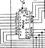
On E6 are 23 and 12 supposed to be shorted together? And if so are they shorted with a trace or a jumper or on the IC?

This feels like a silly question but my board is generating a bad vertical sync signal and I've traced it back to E6.23, E6.12 not being shorted together. I don't see the trace that connects them on the board but maybe its below the IC. Either way before I start shorting things together that I feel should already be connected I wanted to come to yall for a sanity check.

Background (A long winded unnecessary online cooking recipe esq story. You can ignore this and still be able to answer the question):
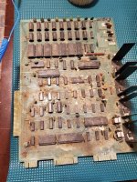
Bought this pet awhile ago at an estate sale non functioning. Got inside it and found out rats had been living in the board along with a bunch of bugs. Spent a ton of time trying to clean the board as esd safe as I could but eventually lost motivation and went onto other projects. Started working on it again recently. New to working on PETs and old computers in general but I've been having fun.
Issue: When it powers on the CRT shows a solid horizontal line.

Power rails - Fine
8MHz clock - Fine
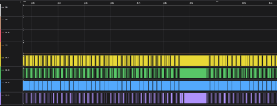
Vertical Drive Output on the PCB - Wayyyyy faster then 60Hz see "Video Signal.png"
Video Signal.png
I then started going down the signal that generated the Vertical Drive output with a logic analyzer on each IC. Since its a repetitive signal I just watched the inputs/outputs and compared them to their logic tables to see if they were "good".
I can post scope captures if wanted but I determined that these signals were "Good"

D8 - 11,12,13
B6 - As a whole
C7 - 1,3,2,4,12
C9 - 1,2,3,9,8,11
^Well idk how much attention I paid to 2/3
C6 - 11,12,13
^Pin 13 Seemed to be on all the time so I started exploring down that route. Throwing Pin 13 high all the time on the falstad simulator generates the same vertical sync issue that I am experiencing.

Then I got to D8 which comparing to the falstad simulation felt like it had really wrong inputs
D8-3-6.png
Tackling them one at a time I started exploring up E8. Pins 1,2,5 and 4 were high all the time. All its inputs.
E8-6.png
So then I looked at the E6 latch that feeds it and saw that the latch that feeds it. The second latch on the IC. Isn't latching. I don't know why E6.7 is showing low when it was high in the feed to E8. Im guessing I hooked one of them up wrong for the capture will scope again when I get home.
E6-Latch-2.png

Which then I looked at the latching signals for E6 and forgive me I forgot to get the scope capture. Will get another one tonight when I can work on it again. But Pin 23 (G1) had a signal going to it and pin 12 (G2) didn't. This makes sense because the second latch the IC isn't latching. Then when I check continuity between the two they are not shorted together. Which is weird because they show shorted together on the schematic but I can't see the trace connecting them when I visually inspect the board. I was wondering if jumpering them is fine or if I'm missing something?
E6-Latch-Schem.png
 
Id say those sockets are probably going to be a hurdle. Judging by the rust youd be lucky to remove sll the ics and keep thisr legs. But the board is certainly salvageable. Good luck and keep us posted!
 
Id say those sockets are probably going to be a hurdle. Judging by the rust youd be lucky to remove sll the ics and keep thisr legs. But the board is certainly salvageable. Good luck and keep us posted!
Yah I did some work on the sockets already which was probably a mistake incase I introduced another issue to the equation. Especially since nothing in my debug has even touched a socketed IC in this chain yet. But I did have a rusted leg fall off on me. I soldered on a leg I snipped off some garbage ICs I have at the lowest temp I could. Looks like its sitting well in the socket but who knows.

Interesting to see how bugs made nests under the sockets lol.

And thankyou!
 
As these are your first posts, welcome to VCFED.

Yes, the two pins in question are supposed to be connected together by a PCB track somewhere.

It is not surprising that a PCB track (or more...) has not been damaged I am afraid.

QDOS for taking this board assembly on though :)!

Dave
 
As these are your first posts, welcome to VCFED.

Yes, the two pins in question are supposed to be connected together by a PCB track somewhere.

It is not surprising that a PCB track (or more...) has not been damaged I am afraid.

QDOS for taking this board assembly on though :)!

Dave
Thankyou. Yah my very very limited electrical engineering experience has been mostly debugging new boards. So a trace going without any signs of heat was a failure mode I wasn't expecting. I appreciate the sanity check
I'm sure Ill patch this trace and it'll boot right up.... right... right? XD

I'll make sure to post the progress.
 
If PC batteries or electrolytic capacitors leak, they eat copper PCB tracks.

Likewise, unhealthy liquids (!) will probably eat copper PCB tracks as well.

Dave
 
The jumper didn't fix it. Same issue. E6 still doesn't seem to be latching G2 properly even with the signal. And I looked further upstream and D6 doesn't appear to be counting correctly despite it getting a proper clock input. Don't have time to debug the issue fully at the moment and will be going out of town till next Monday. So just ordered spare 74177s (E6) and 74100s (D6) incase it ends up being either of those. Obviously wont replace them until ive verified they are the reason its going bad. Just they are cheap and i'll be impatient if I come back and find out I just need to swap them. lol.
 
This board of yours will be a challenge.

For this one I would very carefully remove everything from the pcb, with a good temperature controlled soldering iron and a good solder sucker, a high volume one shot one made by Hakko. You will have to add fresh solder before doing it, as the corrosion on the solder surface tends to act as a thermal insulator.

Then after all of the IC's and sockets and components are removed from the board, wash the board. It ls likely that most of those sockets have a type of plastic shroud that can lift off, meaning the pins can be un-soldered 1 by 1, then the holes solder sucked.

I don't normally recommend the dish washer for a populated pcb, but it will work well on a blank pcb, if all of the components are removed from the board. Then carefully inspect the board for any defects. If the board surface looks tatty & irregular , rub it down with some Innox MX-3 on a cloth, that will restore its original appearance.

Then fit all new sockets, including to the positions where the IC's were not socketed originally. Replace all the resistors and bypass caps.

Clean up the removed IC pins (that were previously soldered in) using solder wick to make sure no solder of any significant thickness remains on the pins, as they will be going into the new sockets. If you have an IC tester, test as many as you can to screen out any obvious duds. Any IC's without excessive pin corrosion may well be ok. Replace all the passive parts with new ones. If the soldered in IC's had their pins trimmed down, you could solder them back in, but I would probably buy new ones and fit them to sockets in this case. You could leave the power rectifiers in place and possibly the voltage regulators, but in my experiences the thermal compound will be degraded and powdery and better replaced. Though they may be riveted in, but you can drill the rivets out.

If the above seems too extreme, it really depends if you want the repair to have long term reliability. I have seen pcb's in this condition "patched up" without a thorough repair, but there is a warehouse full of Steven Spielberg's Gremlins remaining, waiting to rear their ugly heads, if its not done well in the first place. If you do what I'm suggesting you can make the board look new and be reliable again.
 
Last edited:
This board of yours will be a challenge.

For this one I would very carefully remove everything from the pcb, with a good temperature controlled soldering iron and a good solder sucker, a high volume one shot one made by Hakko. You will have to add fresh solder before doing it, as the corrosion on the solder surface tends to act as a thermal insulator.

Then after all of the IC's and sockets and components are removed from the board, wash the board. It ls likely that most of those sockets have a type of plastic shroud that can lift off, meaning the pins can be un-soldered 1 by 1, then the holes solder sucked.

I don't normally recommend the dish washer for a populated pcb, but it will work well on a blank pcb, if all of the components are removed from the board. Then carefully inspect the board for any defects. If the board surface looks tatty & irregular , rub it down with some Innox MX-3 on a cloth, that will restore its original appearance.

Then fit all new sockets, including to the positions where the IC's were not socketed originally. Replace all the resistors and bypass caps.

Clean up the removed IC pins (that were previously soldered in) using solder wick to make sure no solder of any significant thickness remains on the pins, as they will be going into the new sockets. If you have an IC tester, test as many as you can to screen out any obvious duds. Any IC's without excessive pin corrosion may well be ok. Replace all the passive parts with new ones. If the soldered in IC's had their pins trimmed down, you could solder them back in, but I would probably buy new ones and fit them to sockets in this case. You could leave the power rectifiers in place and possibly the voltage regulators, but in my experiences the thermal compound will be degraded and powdery and better replaced. Though they may be riveted in, but you can drill the rivets out.

If the above seems too extreme, it really depends if you want the repair to have long term reliability. I have seen pcb's in this condition "patched up" without a thorough repair, but there is a warehouse full of Steven Spielberg's Gremlins remaining, waiting to rear their ugly heads, if its not done well in the first place. If you do what I'm suggesting you can make the board look new and be reliable again.

You are right. The cleaning I have done hasn't gotten everything off and if I want to really make it reliable I should go with your method. I do have access to great rework stations at my work. The copper planes in the power supply look scary but not impossible. Also hearing that the sockets might be able to be taken off a pin at a time sounds promising to make the de soldering easier. Even if they can't though ill just snip the legs from the body if I'm replacing the socket anyways.

Your method doesn't seem too extreme in fact it would probably have been the faster method if I had started with it. I'm a little torn because I'm having fun doing it in circuit at the moment. Don't get to mess with logic gates at work and, while inefficient, tracing signals down the chain has been really helping me understand how the PET works. I think I might bang my head against the wall debugging it in circuit for a little bit longer then fall back to your method when I give up or after I get it functional again to actually make an effort to preserve it. So whatever kid gets it from my estate sale in 60 years can bang their head against the wall with a logic analyzer too. And thus the cycle of pain continues XD.

Good note on replacing non socketed ICs with sockets also. I'm putting some on order.

Also IC testers aren't a tool I've messed with before do you have a recommendation?

Thank you for the input! Its a good approach.
Don
 
>>> Also IC testers aren't a tool I've messed with before do you have a recommendation?

You get what you pay for I am afraid...

Dave
 
I'm not particularly big on IC testers myself. Generally the best place to test an IC is in the circuit that was designed around it. They can be a rough and ready screening tool, to screen out total duds from a batch of IC's, much like tube testers, but you cannot be guaranteed that all of the possible logic combinations are checked, for example counters with load functions. So I don't rely on testers at all, except to screen SRAM and DRAM chips. Even then not reliable. One tester I bought reported an entire batch of DRAM defective, they were fast parts, worked fine in the computer though. Unfortunately since many Testers appeared on ebay, they have been very foolishly deployed as a "service tool" by some. People have done things such as un-soldering all of the IC's on a board, putting them in the tester and putting them back on the board, in a misguided attempt at fault finding, because it takes less mental effort and skill than having to understand the circuitry and fault find with the scope. They just end up ruining vintage pcbs sadly.
 
Some of the 'cheap' testers do not do a particularly good job of testing some ICs (as Hugo has already stated).

The test vectors (for the logic) are not necessarily 100%. Unfortunately, they do not describe what they do test and what they do not.

Some testers also just give you a GO/NOGO indication rather than what actually failed.

The other thing they do not do well is test at 'full speed' or at parameter extremes (e.g. minimum and maximum voltage).

Obviously, the more professional kit will do more, but cost more...

Dave
 
I'm not particularly big on IC testers myself. Generally the best place to test an IC is in the circuit that was designed around it. They can be a rough and ready screening tool, to screen out total duds from a batch of IC's, much like tube testers, but you cannot be guaranteed that all of the possible logic combinations are checked, for example counters with load functions. So I don't rely on testers at all, except to screen SRAM and DRAM chips. Even then not reliable. One tester I bought reported an entire batch of DRAM defective, they were fast parts, worked fine in the computer though. Unfortunately since many Testers appeared on ebay, they have been very foolishly deployed as a "service tool" by some. People have done things such as un-soldering all of the IC's on a board, putting them in the tester and putting them back on the board, in a misguided attempt at fault finding, because it takes less mental effort and skill than having to understand the circuitry and fault find with the scope. They just end up ruining vintage pcbs sadly.
Gotcha glad to see the pcb looks bad enough to break your usual don't desolder everything rule XD


Some of the 'cheap' testers do not do a particularly good job of testing some ICs (as Hugo has already stated).

The test vectors (for the logic) are not necessarily 100%. Unfortunately, they do not describe what they do test and what they do not.

Some testers also just give you a GO/NOGO indication rather than what actually failed.

The other thing they do not do well is test at 'full speed' or at parameter extremes (e.g. minimum and maximum voltage).

Obviously, the more professional kit will do more, but cost more...

Dave
Understood.
 
When we downsized the office (post Covid), a lot of professional equipment (including chip testers and logic analysers) found a home in my home...

Dave
 
Gotcha glad to see the pcb looks bad enough to break your usual don't desolder everything rule XD


Understood.

It probably is the worst PET pcb I have ever seen, and all rules are made to be broken at some point. Of course my rule would be referring to a pcb in basically good physical condition, and to quote Picasso: "Learn the rules like a pro, so you can break them like an artist"

Once something gets to a certain condition, it can be better to strip it down and re-build it entirely as its the only way to get it back into good order.

Here is a 1939 English HMV-904 TV set I restored, if you look at the before and after photos you can see why it had to be rebuilt:

 
Got everything on order so I should be able to hit the ground running when I get back in STL next week assuming my scope readings do end up showing either the Latch or counter are dead.

An HP Signature Analyser is an intetesting piece of equipment...

Dave
I live for when our lab manager wants to downsize. Luckily I'm the only engineer in the office that likes to tinker in their free time so I get funneled all the old equipment from the lab/stuff from other engineers basements.
My fav was my bosses boss giving me a "broken" Davinci DV55 which just needed its battery terminals dremeled uh cleaned I mean cleaned (don't worry they were fully removed before doing that).
380044759_1026759382084180_3549249149596170809_n.jpg380320846_597387689029407_1469305617432782605_n.jpg379117554_342984894816389_9058204804686008225_n.jpg
Ooh Signature Analyzers look cool. Never messed with one before but reading up on it they look useful.


It probably is the worst PET pcb I have ever seen, and all rules are made to be broken at some point. Of course my rule would be referring to a pcb in basically good physical condition, and to quote Picasso: "Learn the rules like a pro, so you can break them like an artist"

Once something gets to a certain condition, it can be better to strip it down and re-build it entirely as its the only way to get it back into good order.

Here is a 1939 English HMV-904 TV set I restored, if you look at the before and after photos you can see why it had to be rebuilt:

Oh jeez that's an impressive restoration. Congrats! Ill stick to my digital signals 😅
 
Looking at the latch with a scope instead of a logic analyzer it looks like all the inputs are stuck at like 1.65V which is below what it considers the minimum "High" of 2V.
Its voltage rails and clock signals look fine. None of its inputs look like they are <1M ohm resistance to ground while off.

image (3).png

The counters that feed it, D6/D7, have the same issue on their outputs which makes sense because they are feeding it. But their Clock1s, Loads, and CLRs read correct (Well incorrect based off of normal operation but theoretically correct based on the vertical sync being generated). Clock2s are of course bad from being tied to the latch inputs.

There are also three multiplexers directly on the nets in question and depending on the signal they could connect outwards from there to other ICs

E8 also has a input directly connected to one of the bad nets.

There are a good amount of chips on these bad nets and I don't know how to really determine which one is the bad one fully in circuit.
But i'm gonna start with the E6 latch because its the only single chip that could cause every failure. All other explanations would require atleast 2 ICs to fail. I pulled it and am gonna breadboard it to see if its an obvious dud before replacing it when that part finally arrives.

It doesn't look like any damage could be caused by running the circuit without the latch present? So I might also run it with the latch depopulated too see if the counters start counting again. Or if something else was an issue.

The through holes are also bigger relative to the pin then some of the ones we use at work which is putting me more at ease about all the desoldering in my future 😅

Also sad my Saleae can't trigger at the same minimum high signal as these operate at. I still think its useful for quick debugging but ill need to remember to scope when things aren't reading right.

Thankyou,
Don
 
Back
Top