• Please review our updated Terms and Rules here

Pet 2001N horizontal line

Or Can we temporarily deselect the RAM with a jumper?

I'm not sure if this is relevant. On my 2001 PET, the entire DRAM banks can be read disabled by connecting pin 10 of IC G7 to ground, called TP3 on the schematic. But there seems to be a lot of PET board variations.So it would pay to check the correct schematic. On my PET board the read-write 74LS244 bi-directional DRAM buffers are I11 & I10.
 
We shouldn't need to disable the DRAM on this machine because we have physically removed the data bus buffers between the CPU data bus and the DRAM and VIDEO RAM so it can't (or I should say shouldn't) affect the CPU.

Dave
 
Update:
if i try reset many times the machine with c68 short , i can see the correct first pettester screen...but is stucked :(
 

Attachments

  • 1674294535948..jpg
    1674294535948..jpg
    2.5 MB · Views: 5
So how did you get that?

What state is the PET in?

It is no good telling me what you see on the screen without defining what chips you have physically plugged into where.

Also, what is the state of CPU pin 7 (SYNC)?

Dave
 
It is no good telling me what you see on the screen without defining what chips you have physically plugged into where.
I have the same configuration, UD9 and Pettester with E9 and E10 in socket...Cpu pin 7 always low signal :(
Maybe bad C68 or Ne555??
 
So, if the CPU pin 7 (SYNC) is LOW - the CPU has stopped executing instructions. It clearly was running at some point (in order to display the initial PETTESTER screen) but then the CPU stopped working (probably because it received a KIL instruction from somewhere and HALTED). It could do this either by misreading the PETTESTER ROM - or randomly branching to somewhere that is not in the PETTESTER.

Incidentally, we were at this point many posts ago...

We also discounted C68 and the NE555 even more posts ago. A simple test - measure the voltage on the CPU pin 40 (/RESET) and it should stay LOW for about a second after you apply power to the PET. The better way is to measure the voltage on CPU pin 40 and then short out C68. Pin 40 should go LOW for approximately 1 second. If this occurs - C68 and the NE555 is OK and you strike it off our list of things to check.

The reset circuitry will top the CPU starting up correctly in the first instance if it never goes LOW (on CPU pin 40) after the power supply and clock are working. If the CPU starts working, and CPU pin 40 is HIGH, the reset circuitry should not cause the CPU to stop executing instructions...

After the power supply and the clock - the next test on the list should be the reset circuit. This is why we perform tests in a logical manner and rule these things out one at a time.

Can we now go back to our train of though from last night please?

Dave
 
Multiple presses of your reset button (shorting out C68) just causes the CPU to "have another go" at trying to correctly execute the PETTESTER code. My educated guess is that sometimes the CPU halts after a short while, but (sometimes) it manages to get far enough to display something useful on the video screen to let you think it is working - but then the CPU halts again...

This would usually indicate a faulty IC socket or bad soldering, PCB track or something similar.

However, it could also be an IC 'on the edge of operation' or some sort of resistive, capacitive or inductive effect between (say) the data or address bus lines. However, in this case, you can't analyse this sort of problem with the whole PET - you have to break the problem down into smaller (and more manageable) 'chunks'.

Randomly removing ICs and testing them will probably not indicate this sort of issue at all. The IC testers only (generally) check the logic function and not the timing of the ICs. For this type of test equipment you would be paying tens of thousands of dollars!

This is what we were attempting to do last night. Remove all of the influences on the data bus by removing the VIA, PIAs, ROMs and the buffers E9 and E10 and using eight off 1k resistors to simulate a NOP instruction on the data bus itself. If this works RELIABLY we can then move on to the next step of our analysis - having removed the data bus itself from our list of things to check...

Dave
 
This is what we were attempting to do last night. Remove all of the influences on the data bus by removing the VIA, PIAs, ROMs and the buffers E9 and E10 and using eight off 1k resistors to simulate a NOP instruction on the data bus itself. If this works RELIABLY we can then move on to the next step of our analysis - having removed the data bus itself from our list of things to check...
So need i remove e9 and e10 and using 8 resistors on??
 
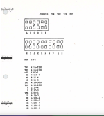
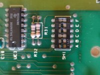
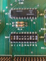
I am desperate because the jumpers don't corresponding to my board!!
 

Attachments

  • Screenshot 2023-01-21 alle 14.57.56.png
    Screenshot 2023-01-21 alle 14.57.56.png
    165.1 KB · Views: 4
????
 

Attachments

  • 1674309547819..jpg
    1674309547819..jpg
    3.3 MB · Views: 3
  • 1674309574931..jpg
    1674309574931..jpg
    1.2 MB · Views: 3
I am desperate because the jumpers don't corresponding to my board!!
At this point in time this is yet another distraction.

These links have no bearing on the fault we are currently tracking down.

Concentrate on the problem at hand rather than getting distracted by other things. By all means note things that look wrong and report them - but don't get distracted by them unless they are significant.

Yes, remove the buffers from E9 and E10.

Put the 1k resistors into IC socket UD8. The data pins are 9-11 (D0-D2) and 13-17 (D3-D7) respectively. Wire the other ends of the resistors to +5V (UD8 pin 24) or 0V (UD8 pin 12) as follows:

NOP = $EA = 1110 1010

D0, D2 and D4 to 0V.
D1, D3, D5, D6 and D7 to +5V.

Dave
 
That is correct. In fact, you should have no ROMs fitted at all (apart from the character generator that is)!

The resistors you have fitted are generating a permanent NOP instruction back to the CPU (exactly as the NOP generator does)...

Dave
 
That is correct. In fact, you should have no ROMs fitted at all (apart from the character generator that is)!

The resistors you have fitted are generating a permanent NOP instruction back to the CPU (exactly as the NOP generator does)...

Dave
Ok danke Dave, so what do i do now?
 
Power it up and check for smoke :)!

Check CPU pins 26 through 33 with your logic probe and post the results.

Check CPU pin 7 for pulses and post the result.

Just to confirm, you have installed one end of the eight 1k resistors into the data bus pins of the UD8 socket (pins 9 to 11 and 13 to 17). The other ends of these 1k resistors are connected either to +5V or 0V. We will check whether they are connected correctly with the logic probe test in this post.

Dave
 
Just to confirm, you have installed one end of the eight 1k resistors into the data bus pins of the UD8 socket (pins 9 to 11 and 13 to 17). The other ends of these 1k resistors are connected either to +5V or 0V
Yes, pins 9 to 11 to pin 12 and pins 13 to 17 to pin 24 (UD8)
 
Yes, pins 9 to 11 to pin 12 and pins 13 to 17 to pin 24 (UD8)
Unfortunately, that is not what I asked you to do back in post #291.

Let me write it out long-hand:

What I am talking of here by (e.g. UD8 pin 9 for D0) is the other end of the 1k resistor that is plugged into UD8 pin 9 be connected to the specified voltage source and not the UD8 pin 9 itself. Is this clear?

D0 (UD8 pin 9), D2 (UD8 pin 11) and D4 (UD8 pin 14) to 0V (UD8 pin 12).
D1 (UD8 pin 10), D3 (UD8 pin 13), D5 (UD8 pin 15), D6 (UD8 pin 16) and D7 (UD8 pin 17) to +5V (UD8 pin 24).

Dave
 
Back
Top