• Please review our updated Terms and Rules here

PET ROM/RAM replacement board

Another idea for lowering chip count would be instead of sending RAM dumps over the serial port, they could be written as files to the SD card.

gubbish,
I like the idea of a serial port because results of the diagnostic tests could be sent to a PC or a display terminal. This would be a great feature if the PET's video is not working (scrambled screen display, etc)
 
You can stop the 6502, but what about the CRTC? IHMO he'd like to access the bus when the 6502 doesn't in order to refresh the screen. So you'd have to synchronize the AVR with the CRTC / PHI 2. Maybe I'm wrong, but please think about it.

I think after the CRT Controller (6545) is initialized with the proper constants during the power up process, it is no longer accessed by the CPU. It simply free runs outputting the proper video timing signals as long as the clocks are running (Phase 1 and phase 2) and RESET is not asserted. I do not think controlling the READY signal will bother it.
 
but now with a possible need for a 'mapping RAM' to do the high speed decode, I agree that it is getting a bit complicated.

Speaking from ignorance, it seems to me that at least in theory adding the "mapping ram" might only increase the parts count by one chip. I'm too lazy to draw a theoretical schematic, but let's imagine the least complicated imaginable implementation:

Use a RAM chip the same size as the one you're actually using for memory. (It's a waste, but there would be compensations. It would make the mapping resolution 1 byte, so if you feel like overriding a single bad memory location or applying a one byte patch to BASIC you could do it.) Address lines are all wired straight through, just like the other RAM. You're only going to need one or data lines to be used as "function selects". (I'd suggest using two. One is the "read/write through" select for the 74LS265, use the other as a "write protect" bit for the onboard SRAM. That would let you selectively map RAM *or* "ROM" into the ROM area.) Those function selects obviously are not on the CPU bus, since the 6502 would never be writing them, only the onboard initialization MCU. You'll need to generate addresses on the MCU for programming the main RAM anyway; that same address generation will work for the mapper. All you'll need is a few more lines from the MCU for writing the mapping RAM's image. (And I mean "a few". If you're only using two bits that's two data lines.)

The same principle applies if you use a smaller RAM; you just map it higher on the address lines, and when you're initializing the memory map you'd just write every Nth bit to map "pages" instead of bytes.

Anyway. Seems to me from a theoretical standpoint at least it's a pretty low-cost way of solving the mapping problem if the MCU can't do it. The board real estate for a RAM chip is exactly equal to that of a DIP switch.
 
Sounds like a good plan with the mapping RAM -
I will have to study what you described with the connection scheme a bit before I fully understand it.
I agree that it would only be one additional chip.
The SRAM chip I was planning on using for the main memory is a Hitachi 68128, which I chose mainly because it was available at Jameco which is a few minutes from my house. :) A second 68128 could be used as the mapping RAM - there was a smaller SRAM available which also looked promising.
 
Mike,
We will need a 32 bit demux because of the requirement to decode a 2K I/O space so that is why Nickolas used a GAL16V8 and a DIP switch to do the job to save room/parts. The guys are trying to come up with a scheme that does not require much user setup other than a simple config file residing on an SD card along with all possible ROM images and let the MCU handle the details but now with a possible need for a 'mapping RAM' to do the high speed decode.
I still don't quite get it; how are you going to configure this map without another working computer, and if you have that computer and a means of dumping RAM and ROM, why would you need a 2K granularity? When E mentions a 1 byte granularity so you can reprogram 1 byte, why would you want to? Just change that byte in your 4K (or 2K) image and replace it all.

Maybe what I need is a sample scenario of how this would actually be used to debug a PET with a bad RAM or ROM chip, a bad data and/or address buffer, etc., that would not require a PC and need less than 4K granularity?

And if you're replacing RAM and ROM and have a serial or USB connection to another computer, why not make it into a real ICE while you're t it?

No, I think the video RAM stays on the main PET board because it needs to time share its bus with the CRT video driver logic. Or are you talking about some kind of shadow RAM of the video on the new board?
No, I just meant that while you're building this main RAM/ROM replacement we'll also need the equivalent of Nicolas' and equivalent video RAM replacement board.
 
how are you going to configure this map without another working computer

the plan is to use an embedded MCU like the ATMega16 to do the configuring of the proper ROM images into a large RAM at power up. A PC will not be needed unless additional debug is desired and is optional.


why would you need a 2K granularity? When E mentions a 1 byte granularity so you can reprogram 1 byte, why would you want to? Just change that byte in your 4K (or 2K) image and replace it all.

Even if all RAM and ROM is to be mapped externally, you still have to map a 2K space internally for the I/O at E800-EFFF.

The one byte mapping resolution is more of a potential capability of the design and probably not going to be used. Do you remember the "trap and patch" schemes for fixing ROM code in the old days?

Maybe what I need is a sample scenario of how this would actually be used to debug a PET with a bad RAM or ROM chip, a bad data and/or address buffer, etc., that would not require a PC and need less than 4K granularity?

Consider a PET with bad RAM or a bad ROM that keeps the PET from running. After installing our new board into the 6502 socket and mapping everything except I/O externally (to the new board), everything works. Now the purest wants to find out where the bad ROM or RAM is to fix the main board and keep things original.

He puts the new board into "Diagnostic mode" by changing a configuration file in the SD card. The new map places code in the F000-FFFF area to pick up the RESET Vector and run test code and maps other ROM space internally to be tested. 2K of RAM is also mapped at external 0000-07FF to have known good zero page and stack space. Hopefully tests indicate what RAM location and/or ROMs are bad.

Of course the space at F000 can not be tested, but if everything else works then the problem must be with the F000 ROM.


And if you're replacing RAM and ROM and have a serial or USB connection to another computer, why not make it into a real ICE while you're t it?

Do you mean a full software development/debug capability with breakpoints, address traps and trigger trace analysis? Now we're talking! Knowing E and gubbish, they are probably capable of doing it!


I just meant that while you're building this main RAM/ROM replacement we'll also need the equivalent of Nicolas' and equivalent video RAM replacement board.

Good point. This will be needed by the original PET guys who are stuck with the 6550 RAMs as a separate little board.
 
Last edited:
I still don't quite get it; how are you going to configure this map without another working computer, and if you have that computer and a means of dumping RAM and ROM, why would you need a 2K granularity? When E mentions a 1 byte granularity so you can reprogram 1 byte, why would you want to? Just change that byte in your 4K (or 2K) image and replace it all.

I guess I'm a little confused myself... In the theoretical board being described there already is another computer: a microcontroller. (Gubbish's choice would be an ATmega.) The idea of this board is rather than requiring the user to program an EPROM with a specific BASIC version (or specific extension/diagnostic ROMs) a single RAM chip is used to selectively replace both RAM and ROM. The ROM images would be stored as files on a micro SD card, and when the PET is powered up the microcontroller will initialize, copy the ROM contents into the correct locations in the onboard RAM, and then reset the CPU. (This would easily let someone, for instance, try multiple BASIC versions, or use the same board in CRTC or non-CRTC PETs.) The reason the idea of a "Mapping RAM" comes up is how to implement the other functionality of the Nicolas board, IE, selective read/write through to motherboard components, page write protection, etc, in an equally soft-configurable way.

For the record, I agree that one-byte resolution is serious overkill. I was just tossing that out there as a "here, you could just do it with two identical RAM chips for a pretty board layout" thought experiment. A perfect size would probably be a 256x4. You'd get four chip selects out of it, more than enough, and 256 byte resolution, enough to, say, only override the zero and one pages of RAM to facilitate running a diagnostic program.

Maybe what I need is a sample scenario of how this would actually be used to debug a PET with a bad RAM or ROM chip, a bad data and/or address buffer, etc., that would not require a PC and need less than 4K granularity?

Without an attached PC it's just as useful as the Nicolas board and more. Since the ROM programming and memory mapping could be completely customized merely by rewriting a config file on the SD card the user could step-by-step run through a series of diagnostic routines which exercise the address lines and data lines (run this while wielding an oscilloscope), test motherboard memory, checksum motherboard ROMs, any number of things.

(Here *is* actually an instance where one byte resolution might be useful, if it were included. You could, for instance, configure a memory map where a 6502 diagnostic program is mapped into empty memory space like 0xA000 and the only part of the system board ROM space that is overridden by the user is the couple of bytes at the top of ROM which hold the power-on RESET vector. That would let the CPU jump straight to the diagnostic program while still allowing it the access to checksum almost everything, including 99.9% of the KERNEL ROM. You could also override a bare minimum of the zero and one memory pages, enough to provide workspace for a complex diagnostic routine, while leaving all the rest of the system memory mapped through for testing.)

A board like this would also be good for development purposes. Having it in a PET would let a programmer develop a completely new 6502 OS from scratch using a cross-compiler on a modern PC and trivially test it by writing a couple files to a card.

In the end, granted, you still need a PC to write ROM images and config files to the MicroSD card, but that certainly doesn't require a PC be powered on in the same room as the PET mechanic. If this is a hangup and you *really* don't want to require another computer to change out what diagnostic routines you're running for a given power-on cycle then I don't see any alternative to having to include some sort of UI with buttons or switches on the board itself, which suddenly makes it much more expensive and complicated.

(Or... I guess, is you could have a program running on the MCU which, using a timer, would step through a series of different memory map and ROM settings, allowing each 6502 diagnostic to run for X number of seconds, after which it would halt the CPU, reprogram memory and passthrough settings, and reset for the next diagnostic.)

And if you're replacing RAM and ROM and have a serial or USB connection to another computer, why not make it into a real ICE while you're t it?

Honestly I sort of agree that the "dump memory contents" bit might be... reaching, and I think you probably are sneaking up on the level of complexity of a full-blown ICE by including it. Frankly I just don't know how trivial it really would be for an ATmega to do the required signal generation at the CPU socket in real time. That seems substantially less easy to me than its other tasks of preloading the contents of a couple of RAM chips and controlling CPU reset. But maybe it's a piece of cake, I don't know.

No, I just meant that while you're building this main RAM/ROM replacement we'll also need the equivalent of Nicolas' and equivalent video RAM replacement board.

That's a separate article, and really needs to remain one. Short of doing something really ugly with a jumper cable there's really no way of incorporating a video RAM replacement onto the same board.
 
One more thought to add,

The memory mapping/configuration and ROM contents on the SD card could be loaded upon MCU startup (via bootloader) into the program memory of the MCU. The ATMega644 has 64k of program memory, so there would be enough to hold the full ROM code along with the program itself. So you could run the board without an SD card until you wanted to change the configuration. Kind of nice to not need the card until you wanted to change things..
 
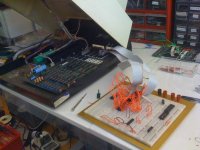
I started breadboarding the RAM/ROM replacement circuit. First I made a cable to bring the CPU socket pins out to the breadboard. That was fun - I melted the plastic around a few of the socket pins so needed to make some repairs before that worked. Now I have a PET 2001 running from a 6502 on a breadboard. The first step was to add a 74LS245 bus transceiver, with direction controlled by R/W from the CPU. Had a little misadventure there since it turned out that the 245 I was using was bad. I did pull it out of an apple IIe which was having issues so it's not exteremely surprising. Perhaps I accidentally found the source of those issues?
In any case, I will get some new logic chips today and continue building the circuit during the week. Just keeping you posted.
IMG_0807.jpg
 
Made some progress on this..
Got a new 74LS245 which worked, and got that working. Then wired up a 628128 128k SRAM, with the chip enable on the 6502 A15 low (lower half of the memory map). Inverted A15 controls the enable of the 245. After a few misplaced wires, success! The SRAM is now acting as the full 32k memory for this PET. Took a few 4116s out of their sockets to check, and indeed removing them from the main board made no difference.
So now I've gotten as far as replacing the RAM. Now for the hard part - connecting the MCU, loading a ROM image into memory, and decoding the addresses.
 
Thanks.. took another small step forward with the project. Added the ATMega644 MCU to the breadboard,
The first thing I wanted to do was to have the MCU reset the CPU.
My initial plan was to hold the 6502 in reset while the MCU loads the ROM code into the appropriate place in RAM, and does all the initialization it needs to do.
After it is ready to go it would raise the reset line on the 6502 and let it run normally.
I connected a pin on the MCU to reset on the 6502, and then wrote a small program to hold reset low for approximately 2 seconds on startup, then bring the line high. It works, sort of. The basic prompt comes up with the normal amount of free RAM, with a blinking cursor. Strangely then the cursor blinks for exactly 9 times, then freezes. When I connect the normal reset line from the board to the 6502 it resets normally.
Didn't have time to figure this out but will look more tonight. Any idea what would cause this behavior?
Thanks..
 
Just as a wild guess about the RESET behavior... doesn't the same RESET line terminate on the 6520s and 6522 on the motherboard? Since the reset line of the 6502 is no longer tied to the other components' reset lines I wonder if something funky could be happening like the 6520 that handles the 60hz timer resets getting angry.

I sort of wonder if a better approach might be to add a wire with a clip that connects to the appropriate leg on the 555 timer to tweak it into firing off a system-board reset instead of just doing the CPU.
 
That sounds reasonable, I think something funky is going on with certain things being reset and others not.
A wire jumper would work, or completely removing the 555 and just letting the MCU reset everything.
This is the 2001 that had some reset issues earlier - and I had actually replaced the 555 with an 8-pin microcontroller (and socket adapter) which just waited a set time and then brought reset high. It's been working fine so far, so perhaps the fact that the other chips are not being reset is causing trouble.
Or if the MCU can do all of it's setup work in the time before the 555 resets the CPU, that might work.. sounds dicey though.
 
I *think* (don't quote me on this) the CRTC PETs also have the CRTC tied to the same reset line.

It's probably a little harsh to expect the user of a final version of the board to have to remove the 555, as of course it's soldered down and the PET wouldn't be able to work stand-alone without it.
 
I agree, definitely too invasive to remove a soldered 555 to get the board to work.
It may be possible to initialize everything during the reset time so the MCU would not need to control that line..
or perhaps the MCU could just halt the CPU with the RDY line immediately upon startup?
 
A bit of further progress to report.
Since resetting the CPU without resetting the other chips was not working, I tried holding the RDY line low for a set amount of time, and then releasing it.
This seemed to work fine - I could even do it repeatedly during a running program and it did not seem to interfere with anything.
So far this seems like the best way to halt system activity while sending debug information over a serial port.

About doing the initial load of ROM contents into RAM -
the SRAM i'm using claims to have an access time of 70ns. I think it is actually a little longer than that, so assuming it's closer to 100ns, that would mean you could load 10 bytes in 10x100ns = 1000ns = 1us. So 10,000 bytes in 1000us = 1ms. Stop me if I'm wrong but it looks like you could load a full 32k in about 3ms? If so then there would not be any need to hold the CPU when doing the preload.
 
Played around further with getting the MPU to act as a decoder to activate/deactivate the replacement RAM.
As many here warned of, it was quite tricky to get the MPU to sync up with the phi2 clock, even running at 20MHz. With the clock running asynchronously the timing was very shaky and while I got close to being able to read the address lines at the right time during the phi2 low phase, it just wasn't working right.
I don't think I'll pursue this route any further - it may be possible but I think it's best to go with the 'mapping RAM' technique and use a second SRAM to act as an addressing decoder. Any suggestions on a particular SRAM that would be a good design choice? Something not completely obsolete/difficult to get would be good. I have several 2114s but those don't seem to be in especially plentiful supply.

In any case I will try out this technique tonight and report my findings!
 
Back
Top