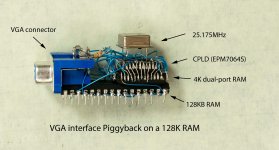
Just for laughs here's my POC. It's a bit more elaborate.
I'm not laughing at all - that looks pretty cool.
I'm in two minds over the Interlace - I can probably fit it into the GAL logic, which would let me access twice the memory for very little image gain. All I need is an external count deciding with bank it will get the frame from... Which is useful for having a video buffer I can write while the other is displaying also.. I just need to adjust the sync timing in the second GAL if I go that way, which means moving pins as I don't have enough logic terms in a 22V10 to cover doing that on the outside pins - and may need to move sync to the middle pins. I have no idea why they put 8 OR gates in the peripheral pins and 16 OR gates in the middle ones! Anyway the only downside of ignoring the interlace is I miss a line one time in 312 frames and I run at 50.1 Hz instead of 50, so my timing is a little out on vertical...
And the BUS arbitration is interesting. I still have to test my design, but generally I'm running memory clock at 7 MHz, Dot clock at 7 or 14 MHz, and that gives me every second half of the 7MHz cycle for CPU access, which if accessed asynchronously means I shouldn't have to wait more than 210ns for a "slot" to appear to either read or write, and the z80 only reads or writes once per three cycles, so that would theoretically let me run at 20 MHz or close to it - as long as I stretch the read timing by latching the data first opportunity when RD goes low and maintain on the CPU side bus until RD goes high again.
Likewise, a write pulse is going to be somewhere around 30ns or so for a write cycle at those kinds of speeds, so I would need to latch the write data until the timeslot comes around again, though on subsequent writes, it's ready again in 140ns, since a degree of co-incidental synchronisation occurs out of a worst-case read/write scenario, and if not, then it's going to latch the write and it won't be any worse than 210ns. Offering half of the memory time to the CPU and half to the video counters seems like an elegant way of doing it and seems to be reflected in speeds of 70 and 55ns coming out in single-port video-ram chips around 1984.
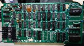
But there seems to be two choices for Myke unless he finds a ready-to-go schematic for a S100 design that he can replicate. ( I'm kind of amazed he has an archive of S100 designs... I never knew such existed. Then again, I never really got involved with S100 back in the day... I ended up going straight to ISA from a small home computer. ). -
The question otherwise, is whether it's better to design a card from scratch using a 6845 or similar, which gives some control over timing, or to do it in logic, with or without GALs or other PLDs, which remove CPU overhead in managing the video circuit, but increases chip count and complexity.
And then the decisions are whether to let the video bus arbitration method generate snow, wait-states or fully arbitrate the bus.
@MykeLawson , I know you like the wire wrap - and your digital logic is pretty good - You could probably design one from scratch to interface with your S100 bus.. And the IDT 4K memory chips are dirt cheap. - eg; the IDT7134SA55P - Which will give you a dual-ported static ram that will connect right up to your other memory access designs, so will be easy to interface and test from your PC.
After that, you don't need any arbitration logic, and you can even forego the buffers since it's only driving a single chip, and then you can build the video driver on the other side of the chip - Just a few counters and some sync generation logic.
If you wanted to keep it really simple, you could generate ALL of the sync timing from a few analog RC timers with potentiometers to adjust the delay and that would provide both sync and blanking, then you could just add in some counters driving the address and shift register directly. If you wanted to go really simple, even the dot clock could be analog and variable in origin. Then you could adjust both position and width via pots. After that, you just need an encoder - but there's plenty of composite output encoder designs around and you could pursue RS170 as a timing baseline.
Alternately, if you use a clock, then RS170 defines a 64uS scan line, which fits beautifully with Base2 timing, so a 12 MHz dot clock means you can use the 8th and 9th bit on the horizontal counter to reset the counter, or a 14MHz dot clock means you can use the 7th, 8th and 9th bit together to reset the horizontal clock, which makes for some pretty clean circuitry and minimal AND/OR with the 9th bit providing blanking, and initial sync timing. You can generate horizontal sync from a combination of bits, or you can just use an analog timer like the Vector Graphics circuit does... In fact, you could copy most of the Vector Graphics circuit and modify it to use with an IDT 7134 and really simplify things... There's no need for the PROM if you do things like generate the timing separately, and use direct counter-to-RAM connection. You can waste the character memory above the 80th character on each line if you like.
The starting point with your own design is to work out what timing you want to use, and whether you want controllable timing (eg, 6845 ) or fixed logic timing.
David