• Please review our updated Terms and Rules here

SOL-20 0909 PATTERN

jon1967us

Experienced Member
Joined
Jul 28, 2022
Messages
91
Location
Los Angeles
Was getting close to normal function, with a Solos prompt and simple operation. Was having some I/O issues, unable to talk to the port externally, or launch the Terminal. Suddenly, after testing voltages on the Personality module and power cycling, I no longer have a prompt or ability to enter characters, only the "9090" pattern.

Here's what's going on:
I get a 909090 with or without the Personality Module.
I've verified supply voltages on connectors.
I have verified supply voltages on the personality connector and on the roms.
Have swapped ram chips between video and processor sections. No difference.
Swapped U23,24,25 with substitutes from spare boards. No difference.

Performed Functional Test No. 1 of CPU circuits. Passed.
"Functional Test No. 2 of CPU circuits." Did not get pattern shown on figure 3-9 in systems manual-only the 090909.

Tested the clock driver, per the manual, and found some anomalies.

Waveforms appeared ok, although not as square as in manual.


From manual:

“At pin 7 of U104 you should measure 8 V dc or higher. (A significantly lower reading indicates a problem
with U104.)”


Pin 7 measured only 3v.


From manual:

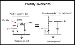
“A 5.1 volt zener diode, D11, and a divider network composed of R130, 131 and 132 derive -5 V dc from the -12 V dc supply for use by the CPU. Diode D12 and the same divider supply -12 V dc to pin 3 of U104, the phase clock conditioner.”

-12v not found on pin 3, U104

Screen Shot 2022-08-12 at 1.38.08 PM.png

Measuring pin 3 and 7 without chip in socket show 0 on pin 7 and -.7 on pin 3

It appears signs are pointing to a bad U104 clock driver, but I'm not getting why no -12v on pin 3. D12 tested ok out of circuit and R132 measures 100Ω in circuit, so no indication of bad components in the divider circuits. Can anyone verify there is -12v on U104/3 from a working unit, as the manual states on VIII-14?
 
Last edited:
Have you verified that -12V supply is normal and arriving at R131 ? If it is then check the voltage at the junction of R131,R130 and R132. That measurement will help determine why there is only -0.7V on pin 3 without chip in socket.

The 0 on pin 7 is probably normal without chip in socket,
 
Have you verified that -12V supply is normal and arriving at R131 ? If it is then check the voltage at the junction of R131,R130 and R132. That measurement will help determine why there is only -0.7V on pin 3 without chip in socket.

The 0 on pin 7 is probably normal without chip in socket,
It’s -6v at that junction. So -12 going into r131 but that resistor drops the voltage all the way down to -6

Couldn’t I at least in Theory jump the -12 all the way to u104/3?
 
Last edited:
Your measurements suggest that D12 or C62 is shorted out to a low R but not zero Ohms, (track shorts excluded) because the voltage is -0.7v there. You will see from the diagrams attached that if pin 3 of the IC got shorted to ground the two 100R resistors R131 & R132 would form a voltage divider down to -6V......The -5V rail will still likely be ok.

One interesting issue is since the days of npn silicon transistors, practically everything went negative earth. So most circuits are better understood in that format.

Positive earth systems (once popular in the 1960's) effectively got re-created when OP amps and other split voltage rail systems and IC's appeared. So positive ground circuitry "messes with some people's heads" myself included.

There is an interesting "trick" which helps people understand positive ground circuits & power supplies. If you have any positive ground system containing diodes, transistors and polarity dependent components, like some capacitors you can :

Reverse the direction any polarity dependent part, like a diode and electrolytic or Tant cap
If there is a transistor npn, switch it to pnp, if there is an pnp then switch it to npn.
Reverse the power supply. Re-draw it in negative ground format (to aid analysis)

This is shown on the attached diagrams. It is a "polarity inversion trick" to help understand how a circuit works in its negative ground format. But you can also reverse real circuits like this too. So when I design using negative power supply rails, I invert the entire design, when its finished I simply flip it back. (it works for discrete designs, not those with IC's)

As you can see with 5v across the zener you end up with 7V across the two 100 R resistors (R131 & R130) in series, or 3.5V across each resistor. So the voltage at the junction of the three resistors would normally be around 8.5V. There would be a small drop across the resistor leading to pin 3 due to the current drawn by the IC, so the IC's pin 3 (all being normal) is expected to be about 8V.

(I didn't draw D12 on the diagrams, but obviously it is in the reverse direction on the two diagrams)
 

Attachments

  • posnegj.jpg
    posnegj.jpg
    110.8 KB · Views: 6
Last edited:
HH, I’ve tested and substituted both D12 and C62 and neither showed leakage nor did their substitution have any positive effect. All three of those 100 ohm Rs in that circuit tests fine.
 
Last edited:
It would be nice to get a little more insight into what exactly is being indicated with the 909090 error. In the meantime, the only thing I can think of is I need to replace U104. Briefly jumping the -6v across R132 or the -12 to D12 cathode, made no difference either. Very mysterious.

One interesting observation was when I inserted a memory card into the S-100 slot. When I turned on the computer the 9090 pattern became an assortment of random characters.
 
Last edited:
With the computer switched off , can you measure the DC resistance (with the IC out of the socket) from pin 3 of it to ground(common).
 
It would be nice to get a little more insight into what exactly is being indicated with the 909090 error. In the meantime, the only thing I can think of is I need to replace U104. Briefly jumping the -6v across R132 or the -12 to D12 cathode, made no difference either. Very mysterious.

One interesting observation was when I inserted a memory card into the S-100 slot. When I turned on the computer the 9090 pattern became an assortment of random characters.
I'm not an expert on this, but I think it (the 909090 error) normally means the personality module is not operational, but that does not necessarily mean the fault lies on the personality pcb. My own sol did this and it was an inverter gate on the main board that had failed.

It is hard to think u104 is at fault, because when it is out of its socket, you don't have about -8v on its pin 3, only about -0.7 you said.
 
My analysis:

You should only be reading -0.7V on pin 3.

-12V is fed to R131 and R132 in series and the -0.7V is derived from the forward voltage drop across diode D12. You shouldn't, therefore be reading -12V on pin 3...

In fact, shorting out R132 would have resulted in an increase in the current flow (and therefore the power dissipation) in D12. Hopefully, it is still OK...

This circuit appears to produce multiple negative voltage rails from the -12V supply. I think Hugo's drawing in the post above accidentally omitted D12.

Do you have an oscilloscope? If so, check the logic outputs on U91 pins 6 and 11. Then on pins 2 and 4 of U104 (after the two differentiating capacitors). And then at the two outputs of U104.

Dave
 
Last edited:
I agree with Dave, I omitted D12 from the diagram I posted, which was silly, because in this Sol circuit D12 is forward biased, so there can at maximum only be about -0,7v on pin 3. And also one would expect about -6V at the junction of the three resistors which is what you are getting.

Looking up the IC's data sheet it can be used with pin 3 connected to a minus supply, or ground, but the designers have chosen to set the voltage at about -0.7v. So it is not clear why the manual said otherwise, but there are a few errors in the sol manual.

The only thing I can think of here is that in the design phase of the Sol, that D12, might once have been intended to be a zener diode (with a reverse polarity to what is shown for the 1N4001) to generate a higher -Ve supply. But in the end they required only about a -0.7V supply , probably so the output stage of the IC swings close to 0v or a little below, so they used the 1N4001 as a voltage reference instead of a zener.
 
Last edited:
@daver2

Thanks for your input. If your analysis is right, which it sounds like it is, that confirmed my suspicions of an error in the manual. Kind of a doozy, too.

Per your suggestion, I’ve scoped those pins.

First are U104/2&4
591797AD-B773-4E05-BC91-A25E7FCC9498.jpeg

55DCF5F4-7FA8-456A-940C-719FB3015503.jpeg
U91/6&11
18C62C98-4313-4D95-88B4-371B6ACBD0A3.jpeg
8A2FEC32-A553-4787-9916-92736D4A2FCB.jpeg
 
My manual is fine... The other end of R131 (that you previously posted and cut off) was connected to -12V.

Those oscilloscope traces look fine to me. What about U104 pins 5 and 7 now (the actual clock signals to the CPU)?

Dave
 
So you have clocks...

Although back in post #1 you stated that U104 pin 7 was only 3V. It looks much better now doesn't it?

What is the lower and upper voltage swing of U104 pins 5 and 7?

I see what you now mean about an error in the manual. I didn't read the (incorrect) words...

Dave
 
Last edited:
I think those phase 1 and phase 2 clock signals out of the IC are ok, Daver2 do you agree ?
Though it would be better if it was a CH1 & Ch2 recording.
 
I think the discrepancy exists because I was measuring DC on pin 7, whereas the scope is measuring a peak somewhere around 8-10v (?)
I'm not sure I can test the swing other than looking at the scope waveform.

I'm starting to think the problem is at the Personality module or the connector. I have 2 P modules and neither works.
Why?
Well, I went back and tested the voltages on the 2708 card, U1, pin 24 and got 4.8v. Fair enough, it seems w/in range.
Next, referring to the manual, which states

"Measure between edge connector pin B14 and pin B15. You should measure more than lM ohms. A reading less than lOK ohms indicates a short."

Measuring between B14/15 I read 80Ω. Which is equivalent of 80Ω from ground to B14
So, I guess the low resistance between B14/15 might be in indicator of a problem at the connector. Further investigation needed.
 
Last edited:
Is the documentation referring to a personality card with or without chips fitted?

Try measuring the resistance with your multimeter probes first one way and then the other.

You could also check C1 and C5 (in that order of probability of failure).

What you are reading is the resistance between 0V (B15) and +5V (B14) so any very low resistance would start to draw a high current. However, 4.8 Volts is only just acceptable. 4.75V is the lower threshold...

Dave
 
You might be on the track of the problem.

Though one interesting thing with the SOL is they are notorious for working and stopping working very frequently because of the TI IC sockets (that most SOLs seem to have) that make poor connections with the IC pins as they grab them across the width on the narrow sides rather than across the flat. It only takes one contact on one IC pin in certain places to go high resistance or open changing the logic state.

One suggestion in the past was to re-seat all of the IC's. Possibly the trouble with this is if you do too many at once and the fault clears, you won't know which socket or pin was responsible.

All the intermittent faults went away in my SOL when I carefully cleaned the sides of the IC pins (every one) and checked every single socket pin with a tool make by soldering an IC pin to a wire handle, to check the socket claw tension, some of the claws were damaged by previous rough insertions of IC's

Though, due to there being a good number of IC's in the Sol, it is not uncommon to get a failure in one or two. As I mentioned the SOL failed in front of my eyes, it was a 74LS04 where is was behaving as though its input pin was open circuit and the gate input assumed a high state inside the IC and its output stayed low regardless of its input state.

At least the process Dave is helping you through should lead to the exact failed IC or open connection to a pin. The worst thing that could happen is if the fault cleared on its own, without knowing why, or where the fault was.

(if you find defective socket claws, you can lift the plastic shell of these TI sockets and gain individual access to the claws)

I cannot recall the details but I think there was a modification done to some of the personality module sockets in some SOL's to accommodate a variant of the module. That would not explain why it was working then stopped.
 
Last edited:
@daver2
I believe I misunderstood and measured the connectors on the PC board rather than the Personality board! :whistle:

The resistance measurements mentioned in the manual are to be performed before the ICs are installed.

Once again measuring between B14/15, connector points, on the P module I get 8MΩ, with no chip inserted.

Note, with a P module inserted, there is data being sent to RAMs U3-10. So it appears the P modules are both sending data

I think next steps will be to follow this data upstream, up through the data input to the CPU and look for faults.

@Hugo Holden
Yes, that's interesting that that's the reputation. It was actually one of the first things I did. Took the ICs out, sprayed the sockets and cleaned the legs with some contact cleaner, as well as clean up the legs with a little Scotchbrite. Every single socket and IC. But, I did not do the insertion test per socket hole. Holy smokes that sounds tedious, but I may take up your suggestion. I'll also check out the 74LS04s.

I'm glad at least the clock section seems to be ruled out. ;)
 
To clean the sides of the IC pins I used a number 11 scalpel blade on a handle. But not the sharp face of it. The other edge is a rectangular section and it is perfect for scaping off the surface oxides without biting into the surface. (it must be the sides of the IC pins, not just their flat faces that have the oxides cleaned off) You require both light and magnification to do it properly. For a 14 pin IC that is 24 surfaces to scape the oxide off and 48 faces for each 14 pin IC, if you also do the flat faces as well (I did because I'm fanatical).

You might note that if you look at these IC pins, when you take the IC out initially, the IC's that have been in those dreaded TI sockets, that there will be a grey or black line where the dissimilar metals of the IC pin and the socket claw have been in contact over decades. These oxides must be scraped off.

After that I finish the surface of the IC pins with 1200 grade paper. It is not a bad idea to lubricate the pins too, I use Inox MX-3 for that. Simply spray some into a shallow container like a Jam jar lid to a depth of 3 or 4 mm, and put the IC pins into that, before re-inserting the IC's in the sockets....of course every socket claw must have been checked without fail with the test IC pin.

And yes, it is very tedious, but it saves a whole world of headaches and intermittent faults later.
 
Last edited:
Back
Top