• Please review our updated Terms and Rules here

Tektronix 4052 Emulator

Dave,

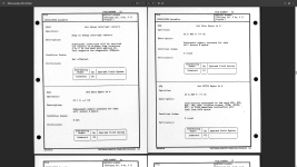
I previously posted this 4052 opcode page including the SFA - Set Fetch Space to A. This page also has instructions to set the Data space to A or B:

1746385491847.png
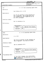
The 4052 TAPX opcode will set ALL the CC bits to the contents of the A register.
Note the Programming note at the bottom - if the F-bit changes the instruction space change will be deferred as in the SFA instruction!
1746385662889.png

The only other way to change the Fetch space is a RTS which will pop the stack copy of CC. But I imagine if the Fetch space is different - the change will be delayed until:

Instructions subsequent to next JSR, RTS, BSR, JMP, BRA, relative branch, RTRN, JMPAX, RTI or FPSH immediate instruction will come from DATA space.
 
Last edited:
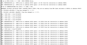
I captured a diagnostic trace of what happens when it all goes sadly wrong again after entering "LIST<RETURN>"

1746385198870.png

Things are going OK up until the WHEREAMI with PC=5C and uPC = 0338. The uPC indicates we are executing the microcode for an instruction 38 (JMPIN). But then it all appears to go sadly wrong. I suspect the "WORD write" diagnostic messages are all part-and parcel of the uCode for JMPIN (hence the "instruction at address 005C" message where the microcode is executing but the "CPU instructions" are not).

Things carry on for a while, and then it almost appears as the the microcode effectively 'resets' the machine and outputs the system error message:

1746385636135.png
Which (if I could decode it) may point me in the right direction?

I don't believe in coincidences, but the fact that RAM memory addresses $005C was (correctly) set to 1 and 0 by instructions at addresses $BAD2 and $BA92 respectively (and these are CORRECT) and then address $005C is subsequently used as a 'program counter' is a bit too coincidental.

I will have a look in more detail tomorrow at what the microcode for instruction $38 (JMPIN) is supposed to be doing.

No further forwards, but the mist is starting to clear on the path!

Dave
 
The new 4052 opcode JMPIN looks pretty straightforward - a 16-bit address is loaded into the PC from the following two bytes and the CC register is unaffected.


JMPINJMPIN addr16EXT3$38?For 4052/4054 & A:


[PC]
[M,M+1]

[CC] unaffected
Jump Indirect


The next instruction to be executed is to be found at the 16-bit address POINTED to by the 16-bit Operand
 
It looks pretty simple - but I think I may have found out what is going wrong. There is something 'special' regarding the use of two bits for this (and other) instructions within ROM U210.

I can see where the microcode machine is not working - and the operand is using whatever 'rubbish' was left in a particular register from the last instruction (hence the microcode is erroneously using the $005C as an operand to the JMPIN instruction and it is all going sadly wrong).

It is getting too late now - so something for tomorrow. Chase bits of wire on the 4052 schematics again...

Dave
 
I have an anomaly...

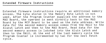
The 4052 technical manual states:

1746556988922.png

This (I take to mean) for any extended instruction that a 2-byte pointer follows the instruction opcode. The data found at that memory location is then used as a 16-bit pointer that points to the instruction operand itself.

However, many other (none 4052 instructions) use EXTENDED mode to reference their operands.

For example, opcode $B6 (LDAA $1000) - that you use in your 4052 opcode table. This clearly does NOT use a level of indirection that the JMPIN instruction ($38) does...

ROM U210 encodes the two instructions as follows:

Code:
Dump of ROM U210.
=================

         7 --------- 8=1 / 16=0.
         |6 -------- FCREAD.
         ||5 ------- EXTENDED.
         |||4 ------ DIRECT.
         ||||3 ----- IMMED16.
         |||||2 ---- IMMED8.
         ||||||1 --- WONFO.
         |||||||0 -- WONFI.
         ||||||||
0x38 ==> .11...11 = ?JMPIN.
0xB6 ==> 111....1 = LDAA.

Having now written this down, I wonder if this has to do with a 16-bit EXTENDED instruction rather than an 8-bit EXTENDED instruction?

A quick look through the U210 ROM identifies the following instructions as falling into this category:

CPX, LDS, STS, LDX and STX.

STS and STX are stores whereas CPX, LDS and LDX are loads (although, in the case of CPX) the value fetched is not actually loaded into a register - just used by the ALU.

The other thing that was 'messing' my emulation up was WONFO and WONFI being set at the same time. I had assumed they would be 00 or 01 or 10, but not 11...

I also now know that IMMED8 and IMMED16 can both be set simultaneously also - signifying an implicit no operation (as far as an operand is concerned).

Tektronix are clearly using some 'illegal or nonsense' encodings to signify 'special' cases - and it is these special cases that are catching me out!

More work to do...

Dave
 
Last edited:
Dave,

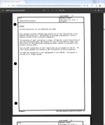
I think Tektronix called ALL the "NEW" 4052/4054 and 4052A/4054A opcodes Extended - see this page in the 4052A Assembler doc:
1746560168026.png
Therefore - this has NOTHING to do with the opcode addressing mode - which is exactly the same as the 6800 - including the A-Series opcodes that require a C7 or FC prefix byte.

The Assembler document lists the processor opcode addressing modes for each of the new opcodes - same as a 6800:

4052/4054 and 4052A/4054A Addressing modes (same as 6800):

ACC
- Accumulator

In accumulator addressing, either accumulator A or accumulator B is specified. These are 1- byte instructions.
Ex: ABA adds the contents of accumulators and stores the result in accumulator A

IMM - Immediate

In immediate addressing, operand is located immediately after the opcode in the second byte of the instruction in program memory (except LDS and LDX where the operand is in the second and third bytes of the instruction). These are 2-byte or 3-byte instructions.
Ex: LDAA #$25 loads the number (25)H into accumulator A

DIR - Direct

In direct addressing, the address of the operand is contained in the second byte of the instruction. Direct addressing allows the user to directly address the lowest 256 bytes of the memory, i.e, locations 0 through 255. Enhanced execution times are achieved by storing data in these locations. These are 2-byte instructions.
Ex: LDAA $25 loads the contents of the memory address (25)H into accumulator A

EXT - Extended

In extended addressing, the address contained in the second byte of the instruction is used as the higher eight bits of the address of the operand. The third byte of the instruction is used as the lower eight bits of the address for the operand. This is an absolute address in the memory. These are 3-byte instructions.
Ex: LDAA $1000 loads the contents of the memory address (1000)H into accumulator A

IDX - Indexed

In indexed addressing, the address contained in the second byte of the instruction is added to the index register’s lowest eight bits. The carry is then added to the higher order eight bits of the index register. This result is then used to address memory. The modified address is held in a temporary address register so there is no change to the index register. These are 2-byte instructions.
Ex: LDX #$1000 or LDAA $10,X
Initially, LDX #$1000 instruction loads 1000H to the index register (X) using immediate addressing. Then LDAA $10,X instruction, using indexed addressing, loads the contents of memory address (10)H + X = 1010H into accumulator A.

INH - Implied (Inherent)

In the implied addressing mode, the instruction gives the address inherently (i.e., stack pointer, index register, etc.). Inherent instructions are used when

no operands need to be fetched. These are 1-byte instructions.
Ex: INX increases the contents of the Index register by one. The address information is "inherent" in the instruction itself.
INCA increases the contents of the accumulator A by one.
DECB decreases the contents of the accumulator B by one.

REL - Relative

The relative addressing mode is used with most of the branching instructions on the 6802 microprocessor. The first byte of the instruction is the opcode. The second byte of the instruction is called the offset. The offset is interpreted as a signed 7-bit number. If the MSB (most significant bit) of the offset is 0, the number is positive, which indicates a forward branch. If the MSB of the offset is 1, the number is negative, which indicates a backward branch. This allows the user to address data in a range of -126 to +129 bytes of the present instruction. These are 2-byte instructions.

Ex:

PC Hex Label Instruction

0009 2004 BRA 0FH


___________________________________________

Since the 4052/4054 have A and B 64KB address spaces - each of which can have executable code in one space and data in the other space, that does blur the 6800 addressing modes descriptions above since the word "memory" in the 6800 is anywhere in the 64KB memory space (RAM and or ROM).


IMM mode for 4052/4054 is clearly describing the operands follow the instruction in the same SPACE as the instruction.

DIR mode on the other hand appears to always require access to the RAM space A for the reads and writes. And the default CC bits Fetch from B and Data in A

EXT parameters are an executable address - so must come from the FETCH space - which could change if the Fetch CC bit previously changed.

I think your microcode emulator needs to exactly match the 2901's and hardware on the boards :)
 
Last edited:
That is what I am assuming. That the EXT addressing mode in the 4052 and 6800 instructions are the same.

However, the JMPIN instruction ($38) does not follow this rule. So there is something else going on within the MCP logic somewhere to differentiate the two different cases.

Dave
 
I am afraid they don't.

The documents describe what the instructions 'do', but not how they do it.

This is encoded in the hardware schematics for the MCP board.

Dave
 
I recall seeing a Tektronix patent granted in 1981 that may have been related to the 4052/4054 memory system design: Memory Access System

The patent describes how to get 16-bits of data that is not word aligned from EVEN and ODD memory banks.
This might be something that happens in the MCP?
 
Dave,

I received a 8.8 million row CSV file 4054 logic analyzer trace from VintageTek yesterday - to see if we can debug why their 4054 hangs with Option 30 - and my 4054 works with their Option 30.

Their trace had these signals:

Bus_[15:0],CH-17 SPACER-1,CH16_ROMCLK-0,WT# CH-18,RST# CH-19

But I don't think the address bus and SPACER-1 is enough to decode the I/O Ports vs RAM, main ROM, bank switch ROM and Constant ROM.

Maybe we need to add another clock to get the I/O ports or RAM??

Looking at the latest Technical Manual and Parts and Schematics - the address decodes for all those devices has more control output bits.

Here is my draft of the control bits and device decoded address ranges taken from those two manuals.

My table of control bits and Device Decoded Address Range may have some errors, since the page descriptions each of the ranges did NOT include all the control bits.

I don't know if this information helps you on the 4052 Emulator - but I would appreciate a quick check of my work before I ask VintageTek to do another trace with a couple more control bits added.

Signal NameFunctionDescription
CONSTROM-0CONSTANT ROM ADDRESSThe enable address of the Constant ROM in the ROM array
MEXT-0M BUS EXTERNAL ADDRESSInstruction decode from the External Address decode on the MAS board, when low, indicates the address is for External data
MSPACE-1MEMORY SPACEThis is the RAM (high) or ROM (low) memory space selection control line from MAS board to MCP board
RAMADDR-0RAM ADDRESS SPACEThis control line from the Address Decode and Data Control on the MAS board indicates RAM space is being addressed
SPACER-1SPACE SELECTThe space control line from the Status Control on the MAS board used to select RAM space (high) or ROM space (low)

DEVICE DECODED Address RangeSPACER-1MSPACE-1RAMADDR-0MEXT-0CONSTROM-0Technical Manual description page / section
RAM (0000-DFFF 56KB)110117-24, pdf 202 / Status Control
I/O Ports (FF00-FFFF)110017-20, pdf 198 / External Address Decode
CONSTANT ROM Space (E000-EFFF 8KB)100107-22, pdf 200 / ROM Control
4052 BASIC ROM (4000-FFFF)011117-14, pdf 192 / Mbus Enable
External BANK Switch ROM (0000-3FFF)001017-20, pdf 198 / External Address Decode
 

Attachments

  • 1746616244027.png
    1746616244027.png
    325.5 KB · Views: 1
Last edited:
The "data bus messing about with logic" is on the MAS board. From a data bus perspective, the MCP board is relatively straight forward.

My 'gut feeling' is that you should be able to deduce what is being accessed from what has been traced. Of course, it would have been much simpler if they had included the signals you have identified.

The problem is that you can only infer what should have been accessed - and not whether it was correctly accessed or not - and this may be part of the fault.

I can take a look tomorrow now. A bit busy today - and just had something else dumped on me that only I can do...

Dave
 
I am (very slowly) starting to make sense of the U210 ROM encodings...

I am currently looking at the encodings of the four (4) bits: EXTENDED, DIRECT, IMMED16 and IMMED8.

The two flags (IMMEDI16 and IMMED8) can take any value from 00, 01, 10, and (the funny encoding) 11.

00 = No immediate operand.
01 = 8-bit immediate operand.
10 = 16-bit immediate operand.
11 = Special condition - instruction does not use immediate data.

When (IMMED16 and IMMED8) = 00 (indicating no immediate operand), then the expectation is that either one (or the other) of the EXTENDED or DIRECT bits will be set (but not both the EXTENDED and DIRECT bits) [i.e. the only valid combinations of (EXTENDED and DIRECT) are 00, 01, and 10 but NOT 11].

If (IMMED16 and IMMED8) are 11 - this activates the IMPNOP-0 signal (Implied no operation) and prevents the activation of the IMPREQ-1 signal (so not activating the Implied Required signal).

No IMPREQ-1 signal means a whole load of logic (that is based upon these various flags above - IMMED8, IMMED16, EXTENDED and DIRECT) are not processed.

{I am a little confused about the descriptions the IMPNOP-0 and IMPREQ-1 signals within the Tektronix documentation. They do not seem consistent with the above description}. IMPNOP-0 goes LOW to indicate that the fetched opcode does not use immediate data {this is the 11 condition action of U265B}. IMPREQ-1 goes HIGH to indicate that the fetched opcode uses immediate data {but if IMMED16 and IMMED8 are 00 then IMPREQ-1 is also HIGH - but the instruction doesn't use immediate data either!}.

There is a signal called USEINDIRECT-0 which is active when IMPREQ-1 is active and EXTENDED-1 is active at the same time. USEINDIRECT-0 cascades into the logic to produce MINDIRECT-0 which seems to kick off the 'magic' on the MAS board to cycle the data that is read from the ROM/RAM back into the address latches and to the re-fetch the data at that address and present it to the ALU in the ALUNIN latches. The microcode then takes over and writes the output from the ALU (that has not modified the data that is presented to the ALU in the ALUNIN latches) to the PC.

I can see how sometimes how the EXTENDED flag is used as per a normal 6800 instruction and sometimes as a 'funny' indirect instruction (i.e. JMPIN). This is all based upon whether a signal called MINDIRECT-0 is active or not.

I need to re-read this again tomorrow and see if it makes any sense whatsoever!

I will also look at how the other addressing modes are decoded on the MCP to ensure I have not missed anything equally subtle as this!

I think I still need to look in more detail at the logic derivations of MINDIRECT-0 and USEINDIRECT-0.

Dave
 
Last edited:
I did a search of the Parts and Schematics for IMMEDI and found a whole page of other unusual signal names on 4-25 (pdf 123): DIRECT_8-1, DIRECT-1, DIRRD8-0, DODIRECT-0, DODIRRAM-0, DOIMD16-0, DOIMD16RAM-0 and DOIMD8-0!

Pages 4-32 and 4-33 have several EXT signal names

Page 4-73 has ZEROOUT-0 and ZEROXFER8-0 that affect the high byte of 8-bit data plus sign extension - which also shows up as a "ZERO HIGH/SIGN EXTENDED" block on the left side of the SYSTEM BLOCK DIAGRAM on pdf page 341

The MCP diagram on pdf page 365 has all those signals plus some PL... signal names on the REQUEST GEN and INSTRUCTION DECODE blocks!

The Technical Manual MCP description from page 7-10 thru 7-15 may help explain some of those signals.
 
Last edited:
I think I have found it!

There is, what appears to be, an insignificant signal sneaking into the MCP logic. This insignificant signal isn't insignificant!

It looks like an EXTENDED addressing mode (as defined for the instruction in ROM U210 with the EXTENDED bit set) is treated as an indirect reference if the microcode contains the bits encoding for "ALU to PC".

There does seem to be a couple of other signals that can affect the above logic that I need to check further.

Interestingly a $7E instruction "JMP (EXT)" is not actually coded as this in U210. It is coded as IMMED-16 not EXTENDED. This seems logical, as the 16 bit operand is stored in the PC, so the 16-bit immediate value is fetched, passed through the ALU unchanged, and then stored into the PC.

I am getting there slowly :)!

Dave
 
I am going to quit while I am ahead today :)!

1746974658249.png

I managed to enter a (very simple) program and list it!

I even tried to run it... but the message about the SRQ is quite insistent...

I haven't fully investigated (or implemented) what I have found out about the JMPIN addressing mode, but I fear there are still some 'gotchas' in there to address...

Still, moving in the right direction!

Dave
 
Great progress!

How does your 4052 Emulator handle the GPIB? Same as the 4051 Emulator?

Interesting that the LIST is somehow also checking GPIB - but I think this is expected behavior as the LIST command supports GPIB devices if you add @d to the command or use PRINT @d,19: where the 19 is the secondary address for the LIST command.

Did you use the latest 4051 Emulator javascript code for anything in your 4052 Emulator?
The Flash Drive code was added to the latest 4051 Emulator and it uses secondary address 19 to return the the File Header that I use to emulate the TLIST command - since 4050 BASIC TLIST only supports the internal tape.
 
>>> How does your 4052 Emulator handle the GPIB?

It doesn't!

Because the memory structure (with the mapping) is somewhat more convoluted that the 4051, and the I/O ports are at different locations etc., I took the decision to leave the old 4051 code in there, but to start afresh with the 4052 I/O code whilst I was implementing the microcode machine.

I am not too bothered at the moment though - because I have not fully implemented what I have gleaned so far about these strange addressing modes and 'exceptions to the rule'. It wouldn't surprise me in the least if I am tripping over another strange artefact.

I already know of one potential issue yet to fix, and there may be more...

I think though (before I go mad and start modifying code) I will add some more diagnostic code to see if I can identify all of the strangeness (e.g. WONFO and WONFI bits set at the same time, IMMED16 and IMMED8 bits set at the same time) etc.

I have just searched the U210 ROM and the microcode for the various 'special mode' occurrences and identified the following special conditions:

Code:
U210 where EXTENDED=1.

         7 --------- 8=1 / 16=0.
         |6 -------- FCREAD.
         ||5 ------- EXTENDED.
         |||4 ------ DIRECT.
         ||||3 ----- IMMED16.
         |||||2 ---- IMMED8.
         ||||||1 --- WONFO.
         |||||||0 -- WONFI.
         ||||||||
0x38 ==> .11...11 = ?JMPIN.
0x7D ==> 111....1 = TST.
0x7F ==> 1.1...1. = CLR.
0xB0 ==> 111....1 = SUBA.
0xB1 ==> 111....1 = CMPA.
0xB2 ==> 111....1 = SBCA.
0xB4 ==> 111....1 = ANDA.
0xB5 ==> 111....1 = BITA.
0xB6 ==> 111....1 = LDAA.
0xB7 ==> 1.1...1. = STAA.
0xB8 ==> 111....1 = EORA.
0xB9 ==> 111....1 = ADCA.
0xBA ==> 111....1 = ORAA.
0xBB ==> 111....1 = ADDA.
0xBC ==> .11....1 = CPX.
0xBE ==> .11....1 = LDS.
0xBF ==> ..1...1. = STS.
0xF0 ==> 111....1 = SUBB.
0xF1 ==> 111....1 = CMPB.
0xF2 ==> 111....1 = SBCB.
0xF4 ==> 111....1 = ANDB.
0xF5 ==> 111....1 = BITB.
0xF6 ==> 111....1 = LDAB.
0xF7 ==> 1.1...1. = STAB.
0xF8 ==> 111....1 = EORB.
0xF9 ==> 111....1 = ADCB.
0xFA ==> 111....1 = ORAB.
0xFB ==> 111....1 = ADDB.
0xFE ==> .11....1 = LDX.
0xFF ==> ..1...1. = STX.

U210 where WONFO and WONFI are both '1'.

         7 --------- 8=1 / 16=0.
         |6 -------- FCREAD.
         ||5 ------- EXTENDED.
         |||4 ------ DIRECT.
         ||||3 ----- IMMED16.
         |||||2 ---- IMMED8.
         ||||||1 --- WONFO.
         |||||||0 -- WONFI.
         ||||||||
0x38 ==> .11...11 = ?JMPIN.
0x6D ==> 11...111 = TST.
0x6E ==> 11...111 = JMP.
0x6F ==> 11...111 = CLR.
0x7E ==> 11..1.11 = JMP.
0xA0 ==> 11...111 = SUBA.
0xA1 ==> 11...111 = CMPA.
0xA2 ==> 11...111 = SBCA.
0xA4 ==> 11...111 = ANDA.
0xA5 ==> 11...111 = BITA.
0xA6 ==> 11...111 = LDAA.
0xA7 ==> 11...111 = STAA.
0xA8 ==> 11...111 = EORA.
0xA9 ==> 11...111 = ADCA.
0xAA ==> 11...111 = ORAA.
0xAB ==> 11...111 = ADDA.
0xAC ==> 11...111 = CPX.
0xAE ==> 11...111 = LDS.
0xAF ==> 11...111 = STS.
0xE0 ==> 11...111 = SUBB.
0xE1 ==> 11...111 = CMPB.
0xE2 ==> 11...111 = SBCB.
0xE4 ==> 11...111 = ANDB.
0xE5 ==> 11...111 = BITB.
0xE6 ==> 11...111 = LDAB.
0xE7 ==> 11...111 = STAB.
0xE8 ==> 11...111 = EORB.
0xE9 ==> 11...111 = ADCB.
0xEA ==> 11...111 = ORAB.
0xEB ==> 11...111 = ADDB.
0xEE ==> 11...111 = LDX.
0xEF ==> 11...111 = STX.

Microcode where FIELD4 = 3 = "ALU to PC".

  FIELD4  = 0x0003. MEMORY CONTROL ... ALU to PC. 067
  FIELD4  = 0x0003. MEMORY CONTROL ... ALU to PC. 06B
  FIELD4  = 0x0003. MEMORY CONTROL ... ALU to PC. 072
  FIELD4  = 0x0003. MEMORY CONTROL ... ALU to PC. 077
  FIELD4  = 0x0003. MEMORY CONTROL ... ALU to PC. 07A
  FIELD4  = 0x0003. MEMORY CONTROL ... ALU to PC. 081
  FIELD4  = 0x0003. MEMORY CONTROL ... ALU to PC. 084
  FIELD4  = 0x0003. MEMORY CONTROL ... ALU to PC. 0AF
  FIELD4  = 0x0003. MEMORY CONTROL ... ALU to PC. 0C1
  FIELD4  = 0x0003. MEMORY CONTROL ... ALU to PC. 0C2
  FIELD4  = 0x0003. MEMORY CONTROL ... ALU to PC. 0CD Fetch instruction.
  FIELD4  = 0x0003. MEMORY CONTROL ... ALU to PC. 0D4 RTSCONT?
  FIELD4  = 0x0003. MEMORY CONTROL ... ALU to PC. 108 PART OF INT STACK REGISTERS ETC.
  FIELD4  = 0x0003. MEMORY CONTROL ... ALU to PC. 119 PART OF RTICONT.
  FIELD4  = 0x0003. MEMORY CONTROL ... ALU to PC. 120 ALTVECT?
  FIELD4  = 0x0003. MEMORY CONTROL ... ALU to PC. 125 ???
  FIELD4  = 0x0003. MEMORY CONTROL ... ALU to PC. 155 JMPAXCON.
  FIELD4  = 0x0003. MEMORY CONTROL ... ALU to PC. 171 FP?CON.
  FIELD4  = 0x0003. MEMORY CONTROL ... ALU to PC. 29A RTRNCONT.
  FIELD4  = 0x0003. MEMORY CONTROL ... ALU to PC. 2BB ???
  FIELD4  = 0x0003. MEMORY CONTROL ... ALU to PC. 2DB ???
  FIELD4  = 0x0003. MEMORY CONTROL ... ALU to PC. 338 JMPIN
  FIELD4  = 0x0003. MEMORY CONTROL ... ALU to PC. 36E JMP
  FIELD4  = 0x0003. MEMORY CONTROL ... ALU to PC. 37E JMP

U210 where IMMED16 and IMMED8 are both '1'.

         7 --------- 8=1 / 16=0.
         |6 -------- FCREAD.
         ||5 ------- EXTENDED.
         |||4 ------ DIRECT.
         ||||3 ----- IMMED16.
         |||||2 ---- IMMED8.
         ||||||1 --- WONFO.
         |||||||0 -- WONFI.
         ||||||||
0x00 ==> ....11.. = ?TRAP.
0x01 ==> ....11.. = NOP.
0x02 ==> ....11.. = ?NOP2.
0x03 ==> ....11.. = ?SFA.
0x04 ==> ....11.. = ?TRAP.
0x05 ==> ....11.. = ?TAP.
0x06 ==> ....11.. = TAP.
0x07 ==> ....11.. = TPA.
0x08 ==> ....11.. = INX.
0x09 ==> ....11.. = DEX.
0x0A ==> ....11.. = CLV.
0x0B ==> ....11.. = SEV.
0x0C ==> ....11.. = CLC.
0x0D ==> ....11.. = SEC.
0x0E ==> ....11.. = CLI.
0x0F ==> ....11.. = SEI.
0x10 ==> ....11.. = SBA.
0x11 ==> ....11.. = CBA.
0x12 ==> ....11.. = ?TAPX.
0x13 ==> ....11.. = ?TPAX.
0x16 ==> ....11.. = TAB.
0x17 ==> ....11.. = TBA.
0x18 ==> ....11.. = ?SDA.
0x19 ==> ....11.. = ?TRAP.
0x1A ==> ....11.. = ?NLDXX.
0x1B ==> ....11.. = ABA.
0x1C ==> ....11.. = ?NLDAX.
0x1D ==> ....11.. = ?NLDBX.
0x1E ==> ....11.. = ?NSTAX.
0x1F ==> ....11.. = ?JMPAX.
0x21 ==> ....11.. = ?SDB.
0x30 ==> ....11.. = TSX.
0x31 ==> ....11.. = INS.
0x32 ==> ....111. = PULA.
0x33 ==> ....111. = PULB.
0x34 ==> ....11.. = DES.
0x35 ==> ....11.. = TXS.
0x36 ==> ....111. = PSHA.
0x37 ==> ....111. = PSHB.
0x39 ==> ....111. = RTS.
0x3B ==> ....111. = RTI.
0x3E ==> ....11.. = WAI.
0x3F ==> ....11.. = SWI.
0x40 ==> ....11.. = NEGA.
0x41 ==> ....11.. = ?FPSHI.
0x43 ==> ....11.. = COMA.
0x44 ==> ....11.. = LSRA.
0x46 ==> ....11.. = RORA.
0x47 ==> ....11.. = ASRA.
0x48 ==> ....11.. = ASLA.
0x49 ==> ....11.. = ROLA.
0x4A ==> ....11.. = DECA.
0x4C ==> ....11.. = INCA.
0x4D ==> ....11.. = TSTA.
0x4E ==> ....11.. = ?FDUP.
0x4F ==> ....11.. = CLRA.
0x50 ==> ....11.. = NEGB.
0x51 ==> ....11.. = ?FSWP.
0x52 ==> ....11.. = ?FADD.
0x53 ==> ....11.. = COMB.
0x54 ==> ....11.. = LSRB.
0x55 ==> ....11.. = ?FSUB.
0x56 ==> ....11.. = RORB.
0x57 ==> ....11.. = ASRB.
0x58 ==> ....11.. = ASLB.
0x59 ==> ....11.. = ROLB.
0x5A ==> ....11.. = DECB.
0x5B ==> ....11.. = ?FMUL.
0x5C ==> ....11.. = INCB.
0x5D ==> ....11.. = TSTB.
0x5E ==> ....11.. = ?FDIV.
0x5F ==> ....11.. = CLRB.
0x61 ==> ....11.. = ?FNORM.
0x6B ==> ....111. = ?PSHX.
0x71 ==> ....11.. = ?STROKE.
0x72 ==> ....11.. = ?EC.
0x75 ==> ....111. = ?PULX.
0x7B ==> ....11.. = ?TRAP.
0x83 ==> ....11.. = ?TRAP.
0x87 ==> ....11.. = ?TRAP.
0x8F ==> ....11.. = ?TRAP.
0x93 ==> ....11.. = ?TRAP.
0x9D ==> ....11.. = ?TRAP.
0xA3 ==> ....11.. = ?TRAP.
0xB3 ==> ....11.. = ?TRAP.
0xC3 ==> ....11.. = ?TRAP.
0xC7 ==> ....11.. = ?TRAP.
0xCC ==> ....11.. = ?ADAX.
0xCD ==> ....11.. = ?WADAX.
0xCF ==> ....11.. = ?TRAP.
0xD3 ==> ....11.. = ?TRAP.
0xDC ==> ....11.. = ?SBUG.
0xDD ==> ....11.. = ?CBUG.
0xE3 ==> ....11.. = ?MVLR.
0xEC ==> ....11.. = ?MVRL.

There is also something about IMMED8 as well lurking when it is used with the "ALU to PC" microcode.

Dave
 
I think I am now confusing two (2) separate things - and assuming they are the same...

DIRECT is an 8-bit operand (as part of the instruction) extended to a 16-bit address, but the instruction can refer to 8 or 16 bit data itself.

Likewise EXTENDED is a 16-bit operand (as part of the instruction) but it can also refer to an 8 or 16 bit data value.

I am merging the two into one (either 8 bit for all or 16 bit for all)...

I need to differentiate between an 8/16 bit address (coming from the instruction) and 8/16 bit data that the address refers to...

Not a thing for tonight though, and I start another business trip tomorrow. Perhaps think about it in the car or the hotel :)...

Dave
 
There is a difference between the documentation saying that the 4052 has an 8-bit A and B accumulator (because the instruction set only uses the A and B accumulators as 8-bit registers) and the accumulators physically being 8-bits.

The registers are stored within the four off AM2901A devices. Each device containing 16 * 4 bits of RAM - the RAM being used as registers.

By default, therefore, the A and B accumulators (which occupy two (2) of the RAM/REGISTER words) are physically 16-bits wide.

I suspect the microcoded MACRO instructions only treat these two accumulators as 8-bits.

I would be interested in seeing where the high bit(s) get set from through... It is possibly the microcode self-test routines?

My error was accidentally using all 16-bits of the accumulators when I should have used only the lower 8-bits. If the power-on self-tests accidentally leaves some bits set in the high byte of the A or B accumulators, then the resulting hardware (and hence my emulation) should have masked these higher bits out. It does now!

I am still hunting through the ROM code to find out where the subroutine is called to set-up the appropriate interrupt table in RAM.

Plenty of false leads...


Dave

From the Technical manual I believe the 4052 high bits of register A and B are set in MCP "ZERO HIGH/SIGN EXTENDED" hardware during the data transfer to the ALU A or B register.
 
Back
Top