• Please review our updated Terms and Rules here

TRS-80 Model II CRT Blurry with Horizontal Lines

The grounding looks ok, probably if its all manufacturer done, but you can still check with the scope. I had not seen inside one of these units before.

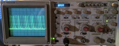
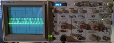
When you are testing it, the video signal at the video card end, also put the scope on the +5V rail that supplies the IC's in that area on the card and check that for noise. I'm wondering if the output from the SMPS is not clean as the signal you measured on the scope looks like RF interference, with components of it, in the 2MHz vicinity, which is unusual if the power supply was clean.

If you put the scope on AC coupling, you can check for ripple on the power supply outputs.

Do you have the schematic for the video card ?
 
Last edited:
@Hugo Holden I deleted a bunch of the traces above because they were (as you suspected) just noise in the ground. I connected a ground wire back to the ground of the scope as a quick & dirty way to filter the noise out. Here's what the signal at the base of Q302 looks like now:

1672690688465.png

Yes there are schematics available in the Model II technical manual. (See numbered pages 71 & 109)

I'll have to do some more probing to look for ripple in the power supply.
 
Last edited:
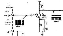
Yes, clearly there were measurement and grounding issues. What you have recorded now, base Q 302 (or Q1 on this schematic), is more representative of the image in the manual on page 103.

I'm not sure about the scope recording with the ripple, is it really on 2V per division ? If it is that is a lot of ripple. It suggests the output filter caps on the psu have gone high ESR, unless there is still a general grounding issue going on corrupting the measurement.
 

Attachments

  • sigs.jpg
    sigs.jpg
    82 KB · Views: 4
Yes, great point about the filter caps on the psu, that's something basic I should have looked at straight away. I have an ESR meter so I'll have a look.

1672746455633.png
 
Last edited:
Firstly the 0.22uF Rfia X2 capacitor is in early failure mode, this is nothing to do with any observed faults you have. Because its casing has split. It is absorbing water and expanding in volume. Sooner or later it will smoke, so at some point in the near future replace it, but leave it for now.

You could check the ESR's in circuit of the electrolytics. Likely the large ones on the primary (line) side will be ok, make sure they are totally discharged before you connect an ESR meter onto those, or they will destroy the meter. Possibly the smaller electros will also be ok, none appear to have domed tops but they could still have dried out.

I would be inclined to put the power supply back in the unit, before doing anything to it, it needs the usual loads to run.

Make both measurements of the DC outputs with the meter and ripple outputs with the scope, for all of the supply's outputs, in case the fault is predominantly on one output. And for the ripple recordings it is important that the scope's ground is connected properly or it could confound the measurements.

One inconsistent thing so far, is that the recording of the voltage at the base of the video output transistor looked normal, it is hard to imagine it could, if there was so much ripple on the power supply. So the ripple recording that you made could still have come about due to some issue with the scope grounding location or something to do with the common connections between the supply and the VDU or the video card & VDU.

For any scope measurements, for this ripple problem, you should post the schematic fragment where you are measuring, and show where the scope earth clip was connected. Also a quick test each time is to short the probe tip to the probe earth clip, just to make sure there is no signal seen , in case the probe earth is defective or intermittent.
 
Last edited:
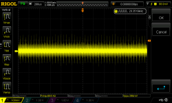
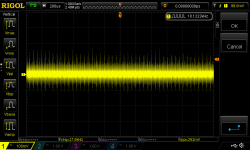
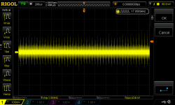
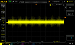
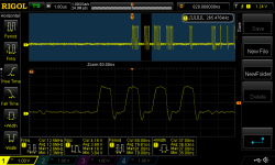
My Christmas present came a week late but finally got here, so I have some better measurements to share. After working with the analog HP it's amazing to use a digital scope. All measurements are taken on the 15 pin PSU connector attached to the PSU PCB, X10 probe AC Coupled. Ground is attached to the body of the metal stand the PSU is mounted on. Like this:

1672885811529.png

5V Rail:
5V.png

12V Rail:
12V.png

-12V Rail:
minus12V.png

24V Rail:
24V.png
 
The supply heatsink body where the scope probe earth is connected, might not be the same as the common lead outputs from the supply, probably the black wires on the connector ? unless there is a direct connection between the two. However the ripple voltages are much lower and might not be unreasonable for that supply, in short the supply may be ok, are its DC output voltages correct ? It is worth checking on the schematic how & where the supply common's get connected to the metal chassis, they usually do but not always. Sometimes it is in the supply, sometimes elsewhere.

Probably reasonable now to go back and look at the video signal at the input and output of the video output transistor and try to find a reason for the smeared video on the CRT image.
 
Last edited:
I checked the continuity between the heatsink body and the black wires and it's about .1-.2 ohms, basically a short so that looks ok. I agree, the ripple looks reasonable.

Here are the voltages measured between the colored & black ground wires on the PCB connector:

ColorBusVoltage Reading (DC)
Red5V4.96
Orange12V12.46
White-12V-12.16
Yellow24V26.16
 
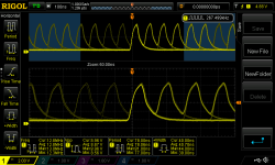
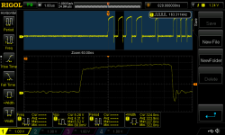
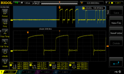
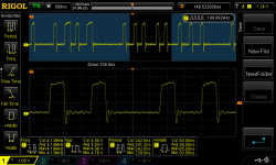
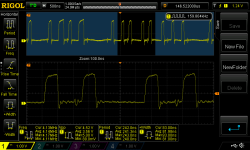
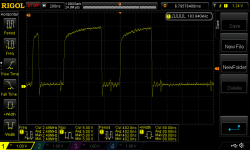
Also, here are some traces from "Point A" at the base of the Q302 Video Amp. I'm thinking these waves (dots on the screen basically) should be more square?

VideoSignal-1.png

VideoSignal-2.png

VideoSignal-3.png
 
Yes, the video pulses look abnormal and appear integrated. While they would not be expected to look perfectly square, they should have faster rising and falling edges.

At least the scope earth looks good and there is no interference.

Just to double check, since I am unfamiliar with your new scope, can you put the Tek scope back on this test point, with similar timebase settings and try with the x10 probe and the x1 probe too, if you have one, and obviously checking adjusting the attentuator to suit that change to get about the same level and we will check that we get the same waveform.

If this is really the signal at the base of the video output transistor, probably the VDU is ok and the problem is on the video card, and we will have to scope that. Do you have another card to try ?
 
Last edited:
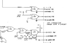
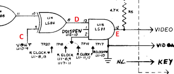
........the video output stage on the card looks simple enough, scope the inputs and output of the 74LS11. Also check what the output on the 74LS11 looks like with the VDU video (link/cable) between the card and the VDU disconnected.
 

Attachments

  • LS11.jpg
    LS11.jpg
    52.3 KB · Views: 3
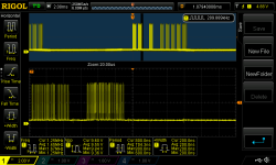
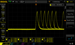
I took some readings on the following points (C, D, E)
VideoCircuit.PNG

Point E (with link cable connected)
PointE-1.png

Point E (with link cable disconnected)
PointE-2.png

Point D #1
PointD-1.png
Point D #2
PointD-2.png
Point D #3
PointD-3.png

Point C #1
PointC-1.png

Point C #2 (this is at the very end of one set of screen signals)
PointC-2.png
 
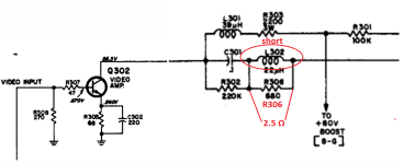
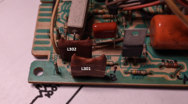
I may have found something. I got to testing all the resistors on the RCA display board in the video signal path. R306 looked like it was shorted, but when I removed the component it checked out ok at 680Ω. It appears there's a short across L302, can these old inductors short out after a period of time? I don't see any other path there. L301 checks out OK.

VideoPath R306.PNG
L301_L302.PNG

Edit: I went ahead and removed L302, it is indeed shorted.
 
Sometimes these low value inductors, in the tens of uH range, can have very low DC resistances. What is the DC resistance of L301 and L302 measured on the Ohms range with the meter ?

It is interesting that the recording at the base of the video output transistor was abnormal, but the output at the IC test point E on the video card looks basically ok, there is the contrast control in between the two points and the cables. Check that the contrast control is basically working and that is ground leg is properly grounded. Check with the meter, the DC voltage on the collector of the video output transistor.

It is acting as though there is additional capacitive loading on the output of the contrast control, in the base circuit of the video output transistor, integrating the signal. This can happen with a defective transistor or open circuit load resistor.

L301 is a shunt peaking coil which raises the impedance in series with the 2.2k collector load resistor R303 (Check this is not O/C), which helps preserve the frequency response of the video amplifier over a few MHz. L302, is a series peaking coil, that is designed to counter the CRT's load capacitance and help preserve the high frequency drive to the CRT. It is a standard combination, as used in most TV sets.

Check a few other voltages too, the voltage across the 2.2k load resistor and check the resistor value, that way we can work out the transistor's collector current. Also measure the transistor's emitter voltage.And check the Boost voltage is in fact 80V.

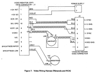
Also to double check, there are two versions of the VDU, Motorola & RCA, one has an additional 270 Ohm base resistor, like yours, so I assume yours is the RCA, but they don't show a contrast control, do you have the contrast control or not or is there just a direct link to the video card?
 
Last edited:
Inductor DC resistance:
  • L301 - open circuit
  • L302 - 2.5 Ohms
Agree about the video card output. This is indeed the RCA board and has the external brightness & contrast pots. The contrast control doesn't do much, but I can see the screen react to it. I checked the ground leg per the diagram on page 100 of the tech ref and it's solid.

1673183346240.png

Q302 Collector Voltage: 69.1V - 69.2V
Q302 Emitter Voltage: .6 mV - .7 mV

R303 looks good and measures 2.263k ohms on the bench. In operation the voltage across it is 74.3V-74.4V on the inductor side, and 74.4V on the 80V Boost side.

Wow thanks for explaining the functions of the inductors in layman's terms. I don’t have a gut feel for things like frequency response and load capacitance yet, but this is a start!

Edit: I was doing some research on "Shunt Peaking" and found a pretty good PDF with some examples. http://www.tscm.com/NEETS-v08-Amplifiers.pdf (Page 2-14)
 
Last edited:
Inductor DC resistance:
  • L301 - open circuit
  • L302- 2.5 Ohms

In operation the voltage across it is 74.3V-74.4V on the inductor side, and 74.4V on the 80V Boost side.
OK, this is the problem. With an open L301 there is no significant collector current and no voltage drop across the 2.2k load resistor. This alters the input conditions to the video amplifier transistor, and makes its base circuit just look like a diode. Then the capacitor in its emitter circuit integrates the input waves, which is why they are corrupted at the transistor's base, but ok out of the video card.

So put L302 back in (as it is ok) and for now just replace L301 with a link wire. (there will be a tiny loss of HF response, but basically it should spring into normal life).

Order a new inductor at some point, this sort of inductor is just fine:

 
Last edited:
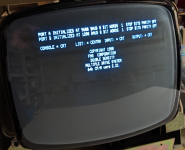
Display smearing is gone, brightness & contrast work as they should now!!!

1673225877331.png

@Hugo Holden TYSM for your help with this. I've learned a ton and thanks to your expertise the video issue is solved.

p.s. does L301 have to be replaced with a "RF Fixed" inductor or would a "Power Choke Inductor" (like below) work as I might have one of those I can replace it with.

1673226392341.png
 
Last edited:
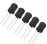
Possibly, the power choke inductor would be ok, though I'm not sure about their self resonant properties. These ones are designed for higher currents, mainly in power coupling applications as series filter elements, rather than in signal amplifier circuits as frequency correcting elements. Also it would likely have a low range self resonance as its winding capacity is likely higher than a wave wound type. You could certainly try it, it may well be perfectly fine.

The type (style) of inductor I directed you to on that ebay link, is typical of many early Miller types, has a small low self capacitance wave wound coil, with fairly thin wire, which has a higher resistance, in the few Ohm vicinity. These are the typical kind of inductors used in video output stages, or other circuits as frequency compensating elements.

Though you might not spot much difference in use, without a detailed frequency response test pattern, even without the shunt inductor at all, except the the text might look just a little softer on its edges without it.

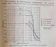
The series peaking coil is a little more important than the shunt coil. To explain this I have attached the standard normalized frequency response & relative gain curves (due to Grob) of shunt & series peaking separately, together and no peaking.

As you can see, if you go from combination peaking (4) as your video output stage has, to just series peaking (3), the bandwidth still remains pretty good and the relative gain only drops down from 1.8 to 1.5, which is more than easily taken up on the contrast control.

If you look at shunt peaking alone (2) you can see how it lifts the response at the high frequency end, which helps to sharpen up the image by improving the detail in the CRT image. All of the fine detail of edges and thin lines on the CRT image relate to the high frequency components in the signal driving the CRT.

These curves explain why, with no shunt coil and just series peaking, it still looks pretty darn good.
 

Attachments

  • Peaking.jpg
    Peaking.jpg
    151.6 KB · Views: 2
Last edited:
Back
Top