• Please review our updated Terms and Rules here
  • From now on we will require that a prefix is set for any items in the sales area. We have created regions and locations for this. We also require that you select a delivery option before posting your listing. This will hopefully help us streamline the things that get listed for sales here and help local people better advertise their items, especially for local only sales. New sales rules are also coming, so stay tuned.

Wanted: bus correction kit for AT&T 6300 (Olivetti M24)

Checked it all again and it looks good, at least until someone else finds the next bug. :)

One thing for you to check - A7 on the 82S147 was tied to GND, and A8 was the bank select jumper. On the new card the bank select jumper is A7, and there is no A8. If you got that right, then it should be good.

Digger, I reread your original post, and I want to check one thing:
It consists of a card and a separate disabler chip for the on-board video board.

IIRC the onboard video can be disabled with a DIP switch, though it may need a newish ROM. Is there some other chip we need to clone to make this thing work?
 
There was one person who has done it with ROM 1.43, never tested on lower. If I had an EGA card I would test it out on the ones I've got, with old rom versions. If someone has one with the newer rom version and can dump the roms we might be in luck.

A while back someone asked me to dump my 1.43 ROMs and I never got around to it because I was busy with another project, but my current project would give me an excuse to retrieve my 6300 out of storage. I don't have an EEPROM reader but I could certainly go into debug and dump f000:000 if that helps. Does someone need me to do that on a 6300 runnins ROM BIOS 1.43?
 
I can provide a 1.43 ROM dump if anyone cares.

As far as disabling the existing video, it depends on the revision of the video card. The procedure for the P8 revision is somewhat different from the earlier revisions, which involve substituting a jumper block for one of the video PALs (which is what got me here to start with--it apparently also works with the P8 card--on mine, someone lost the original PAL). At any rate, the procedure is detailed in the back of the 6300 Service Manual.

I do have a cut a jumper around a couple of the ICs on my bus converter board. Whether or not that's part of the correction mod, I'm not sure. If anyone has the will to do this on their own, however, I can provide details.

Note also, that I have several changes on the main board, as well as the "piggyback" keyboard controller board using the TI MCU--I don't know how that's tied in to the whole affair.
 
@keepiru:

I ran the simulation and discovered that in the process of flipping the chip upside-down, I'd reversed the order of the output bits. Here's the revised pinout. Note that none of the input pins change, but the output pins shift up, with a similar single crossover. Hopefully, this won't mess you up too badly:

Code:
       ._____    _____.
       |     \__/     |
   CLK |  1        24 | Vcc
       |  2        23 | o7
       |  3        22 | o6
    a0 |  4        21 | o5
    a1 |  5        20 | o4
    a2 |  6        19 | o3
    a3 |  7        18 | o1
    a4 |  8        17 | o2
    a5 |  9        16 | o0
    ce | 10        15 |
    a6 | 11        14 |
   gnd | 12        13 | a7
       |______________|

Running the simulation, I get the following output:

Code:
0000  f3 f3 d3 d2 d2 92 d3 db d8 dc 9c 4c 4c 4c 4c 4c 
0010  f3 f3 d1 d0 d4 94 d4 44 44 44 44 44 44 44 44 44 
0020  f3 f3 d3 d2 d2 92 d3 db d8 dc 9c 4c 4c 4c 4c 4c 
0030  f3 f3 d1 d0 d4 94 d4 44 44 44 44 44 44 44 44 44 
0040  f3 f3 d3 d2 d2 92 d3 db d8 dc 9c 4c 4c 4c 4c 4c 
0050  f3 f3 d1 d0 d4 94 d4 44 44 44 44 44 44 44 44 44 
0060  f3 f3 db dc 9c d8 d9 db d3 d2 d2 92 42 42 42 42 
0070  f3 f3 d1 d0 d4 94 d4 44 44 44 44 44 44 44 44 44 
0080  f3 f3 f3 d3 d2 d2 92 d2 d3 db d9 d8 dc 9c dc 4c 
0090  f3 f3 f3 d1 d0 d4 94 d4 44 44 44 44 44 44 44 44 
00a0  f3 f3 f3 d3 d2 d2 92 d2 d3 db d9 d8 dc 9c dc 4c 
00b0  f3 f3 f3 d1 d0 d4 94 d4 44 44 44 44 44 44 44 44 
00c0  f3 f3 f3 d3 d2 d2 92 d2 d3 db d9 d8 dc 9c dc 4c 
00d0  f3 f3 f3 d1 d0 d4 94 d4 44 44 44 44 44 44 44 44 
00e0  f3 f3 f3 db d8 dc 9c dc d8 d9 d3 d2 d2 92 d2 42 
00f0  f3 f3 f3 d1 d0 d4 94 d4 44 44 44 44 44 44 44 44

Which corresponds to the original PROM, but leaves the copyright notice out.

Applicable GAL programming files attached.
 

Attachments

  • busc1122.zip
    2.2 KB · Views: 5
Last edited:
Just in case anyone cares: The BIOS chips on my motherboard are V1.21, the PROM has 'PBFP' on it, and the PALs are not labelled.
 
@Chuck(G):

No problem, it's an easy fix. I just shifted the whole chip down by two pins. You'll need to adjust the address lines as shown.

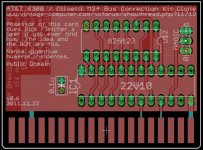
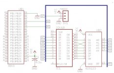
all-v0.6.jpgschem-v0.6.jpg
 
Okay, if this is right, I'll generate a JEDEC file and see what how it burns.
Code:
         ._____    _____.
         |     \__/     |
     CLK |  1        24 | Vcc
      a0 |  2        23 | o7
      a1 |  3        22 | o6
      a2 |  4        21 | o5
      a3 |  5        20 | o4
      a4 |  6        19 | o3
      a5 |  7        18 | o1
      ce |  8        17 | o2
      a6 |  9        16 | o0
      a7 | 10        15 |
         | 11        14 |
     gnd | 12        13 |
         |______________|
 
Yeah, but it's got me wondering...

If I go back to the original PROM, I don't quite understand something.

If the jumper setting was to "disable" the bus correction, we should see an entry of 32 bytes repeated 4 times (i.e. A5 and a6 don't matter). But we don't. In both cases, we see 32 bytes repeated 3 times and a 4th grouping of 32 bytes that's different. So what is the jumper setting supposed to do?

Can anyone read the original PROM (82S123) and tell me what the contents are? It may be simpler to modify the contents of the original PROM using a smaller GAL and keep the PROM with the adapter--and create a "true disable" for the correction.


Sorry for the thinking, but I'm trying to make sense out of this one.
 
I labelled the jumper "Magic" instead of "Enable" for a reason. :)

I looked at it a bit from the other end trying to figure out the pattern. Here's the bitmap of the first 128 bytes:

Code:
0000000 11110011    0000001 11110011
0000010 11010011    0000011 11010010
0000100 11010010    0000101 10010010
0000110 11010011    0000111 11011011
0001000 11011000    0001001 11011100
0001010 10011100    0001011 01001100
0001100 01001100    0001101 01001100
0001110 01001100    0001111 01001100
0010000 11110011    0010001 11110011
0010010 11010001    0010011 11010000
0010100 11010100    0010101 10010100
0010110 11010100    0010111 01000100
0011000 01000100    0011001 01000100
0011010 01000100    0011011 01000100
0011100 01000100    0011101 01000100
0011110 01000100    0011111 01000100
0100000 11110011    0100001 11110011
0100010 11010011    0100011 11010010
0100100 11010010    0100101 10010010
0100110 11010011    0100111 11011011
0101000 11011000    0101001 11011100
0101010 10011100    0101011 01001100
0101100 01001100    0101101 01001100
0101110 01001100    0101111 01001100
0110000 11110011    0110001 11110011
0110010 11010001    0110011 11010000
0110100 11010100    0110101 10010100
0110110 11010100    0110111 01000100
0111000 01000100    0111001 01000100
0111010 01000100    0111011 01000100
0111100 01000100    0111101 01000100
0111110 01000100    0111111 01000100
1000000 11110011    1000001 11110011
1000010 11010011    1000011 11010010
1000100 11010010    1000101 10010010
1000110 11010011    1000111 11011011
1001000 11011000    1001001 11011100
1001010 10011100    1001011 01001100
1001100 01001100    1001101 01001100
1001110 01001100    1001111 01001100
1010000 11110011    1010001 11110011
1010010 11010001    1010011 11010000
1010100 11010100    1010101 10010100
1010110 11010100    1010111 01000100
1011000 01000100    1011001 01000100
1011010 01000100    1011011 01000100
1011100 01000100    1011101 01000100
1011110 01000100    1011111 01000100
1100000 11110011    1100001 11110011
1100010 11011011    1100011 11011100
1100100 10011100    1100101 11011000
1100110 11011001    1100111 11011011
1101000 11010011    1101001 11010010
1101010 11010010    1101011 10010010
1101100 01000010    1101101 01000010
1101110 01000010    1101111 01000010
1110000 11110011    1110001 11110011
1110010 11010001    1110011 11010000
1110100 11010100    1110101 10010100
1110110 11010100    1110111 01000100
1111000 01000100    1111001 01000100
1111010 01000100    1111011 01000100
1111100 01000100    1111101 01000100
1111110 01000100    1111111 01000100

I did not achieve enlightenment.
 
Well, if one or the other jumper setting is best, we can cut down on the complication and fit the whole thing into a GAL16V8, 20 pin chip, which is considerably easier to find than the GAL22V10.

I did some looking around today and finding any small-scale 5 volt programmable logic is getting to be a real problem. The vendors are dropping GALs, ispGALs, PROMs and small 5V CPLDs from their product lines like they were smallpox-infested.

I guess the future is going to be all low-voltage FPGA.
 
Last edited:
Digikey has 22,788 22v10s in stock. 7,677 are DIPs. All the Atmels at least are electrically erasable and reprogrammable (eg a GAL). And if you need more capacity, the 750 is a 22v10 with 2 cells per output (with feedback and more product terms). Lattice dropped them but they look like they are here to stay. I've even used TSSOPs for some combinatorial glue on modern designs.
 
Both are in full production, not NRND.

I'm having a little trouble figuring out what a 32Kx8 bit EPROM has to do with this discussion...

I'd read somewhere (Electronic Products?) not too long ago that Atmel had indicated that the 5V GALs would be in production only until 2014. It'd be great if they continued production past 2014.
 
I'm having a little trouble figuring out what a 32Kx8 bit EPROM has to do with this discussion...

You mentioned it: "The vendors are dropping GALs, ispGALs, PROMs ..."

And it's also a viable option if the PALs don't work out for some reason.
 
You mentioned it: "The vendors are dropping GALs, ispGALs, PROMs ..."

And it's also a viable option if the PALs don't work out for some reason.

I meant small logic PROMs; e.g. Intersil HM-6642(way too slow). The 82S123 is 32x8 bits; the 82S147 is a whopping 512x8 bits--twice what the application requires. Using a 32Kx8 OTP PROM in an 0.600" DIP (128 x requirement) seems to me to be a little over the top, no?
 
On the one hand it's completely overkill... On the other, at $1.08, it's the smallest, cheapest 5v parallel ROM still in production. I go through the same mental loop whenever I go to buy a hard drive and find they've bumped up to the next SI prefix.

What's the advantage of a fuse-programmed PROM over EPROM? I know it's more radiation-tolerant, but it's not often that's a design requirement. :)
 
Last edited:
I'm not sure why a part that has 128 times the required storage disqualifies it from use because it's 'over the top.'. It still meets the storage requirements.
 
Back
Top