bzotto
Experienced Member
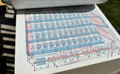
Early micro kits came with (typically) beefy instruction binders, full schematics, and board layout diagrams. Sometimes, red/blue PCB diagrams would be included with the instructions. Attached is one such example apparently from OSI; SWTPC did this too I think in some cases. I know that such diagrams were produced and used in house in as a step in to-scale photolithography of double sided PCBs. But it seems to me that high quality color copies cost money, and the added value of having full red/blues doesn't seem worth much to an end-user who is only assembling a board. Unless the customer was expected to use a high-quality image like this for some sort of photo process of their own? Can anyone--especially someone who was there at the time!-- shed any light on this? Thank you!