• Please review our updated Terms and Rules here

The Sol Prototype Project

MCM6574P keyboard chips

Isn't that a character generator?

Anyway, I guess the point I was making is, well, if you have a "Subsystem B" you pretty much already have a SOL-20; the ROM on the GPM board *is* the "Personality Module", and it seems in principle you could change it out for whatever you want. So for your own needs it'd seem like you'd be covered without building anything?

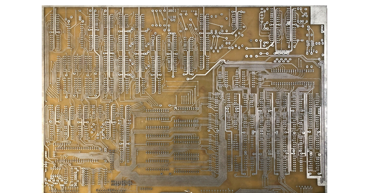
Maybe this is an ignorant way of looking at it, but isn't most of the "secret sauce" that distinguishes a SOL-20 from a vanilla 8080-powered S-100 machine the unique aspects of the VDM-1 video board? I guess I'm wondering if the definition of "reproduction" were expanded to include hardware that used more modern components for availability/chip count reasons what would be the exact level of fidelity necessary to run, say, the majority of the non-CP/M software on Sol-20.org's archive. Or is this all about just churning out a copy of the original PCB board specifically?

I guess maybe it's an interesting thought exercise to ponder how one could make a simplified Sol-20 compatible with "more modern" parts but stopping short of just cramming it all in an FPGA or CPLDs. Looking through the schematic parts of it are *very* obsolete, like the TMS6011 UARTs that are used for both the serial port and cassette interface. (I mean, I guess it looks like maybe the TR1602 might be close to a direct replacement, but that's still long gone...)
 
Last edited:
CHM was kind enough to do that for me personally when I asked.. they did it either just before or just after Al took his pictures. Here's an example: https://drive.google.com/file/d/1cIDV3BKN1ZvXo2JD_4InCzO0qF7Z93dr/view?usp=sharing
Ah OK, I did not know that you had received a photo set with ruler, that's very useful! I'd be interested in seeing these photos myself, if that would be ok?
The reason I ask is that I have also used Al's and Marc's photos for a project by using them as a background, aligning and drawing over them with CAD to produce this

The use of a coin in a photo can be more useful to extract measurements from than a ruler. The coin is placed directly on the surface of the object, or stood on edge against a foreground vertical face. Then a CAD datum line can always be drawn across the coin diameter that is parallel to a desired edge in the photo, even in a perspective shot.

Sure! Anything I have is accessible here: https://drive.google.com/drive/fold...ourcekey=0-LsJ7Ci2Zava5XElbk7VD7w&usp=sharing

I really should learn CAD. I mean, my technique sort of works - I'm lucky that I have almost the exact same keyboard as the original - I can scale based on that alone. But it'd be nice to put it into a CAD program so the people who will do the metal work for me have something easily followed.

Hi,

I use SolidWorks ... IF I have a part in hand, I can 3D model it fairly quickly, do laser etchings onto paper or cardboard to test fits to be as close as the original CAD drawings.


.
 
I had a go at trying to extract some dimensions from the photos supplied to Falter.

I started with IMG_9021 as this seemed good for the panel. This image is 4032 x 3024 pixels (on its side) so I created a new drawing with a bounding rectangle at those pixel sizes in mm to contain the image.
So, 4m x 3m approx. I zoom in to place line points, starting with red to indicate photo features, point to point (eg. half thickness of the top rear sides) projected to a yet-non-determined vanishing point.
After a few lines are done, the (eg. left) VP comes out at about 8.2m to the left. Picking the middle 'sweet spot' of the intersections, this becomes the adjusted VP and all lines are trimmed and tweaked to there.
Next lines are added in blue to indicate from the origin at the VP through to (or past) a new feature.
The ruler is happily well placed in this image, with the divergence angle from the side panel (91.87 degrees) and ruler (91.25 degrees) so 0.62 degrees out out of parallel. So, good for measurements which are in green.
Ignoring the rounding, the ruler 12" mark extends 1/4" past the projected rear vertical edge of the panel. The front edge of the panel extends 5/32" beyond the origin of the ruler. The 1/16" markers for the first inch are mirrored past the ruler origin. So I determine the panel length front-back to be 12-1/4" as the rear vertical edge is slightly concave by 1/16" or so.

The height of the panel appears to be 5-1/4" but it's hard to tell if it was placed at the transition curve from front to top. I took it as that. From the height VP (about 13.4 metres above the image) and projected to the front upper corner, the intersection against the rear vertical gives a ratio of 122.35mm/231.59mm or 0.5284 of the panel height. So, 2.775" but I think it's most likely 2-3/4".

There are lots more dimensions that can be extracted as the cassette is 100.34mm wide (for a standard Australian compact cassette, no idea how big US or European ones are LOL).

SOL_prototype_overdraw1.pngSOL_prototype_overdraw2.pngSOL_prototype_overdraw3.pngSOL_prototype_estimated_side_dimensions.png
 
I used image proto_plex_2 and found the side grid angle for the verticals from IMG_8999 by aligning the screw hole centres from both images (yellow line). I had initially assumed the plexiglass to be 1/4" but from projection lines it seems to be thinner, 2.07mm or approx 3/32" thick. I think. The grid is 1/4" squares. I have extracted some other dimensions for the keyboard and tape cutout. Also, using the marshfelsenstein2 image the side profile above changes only a tiny bit with the angled keyboard edge being just over 3mm higher. BTW I'm just doing this for a bit of fun, hope I'm not bothering this thread. I sometimes think if I went back in time to WWII I would want to be an intelligence photo interpreter more than anything.
SIT_plexiglas_side_profile_estimated.png
 
I used image proto_plex_2 and found the side grid angle for the verticals from IMG_8999 by aligning the screw hole centres from both images (yellow line). I had initially assumed the plexiglass to be 1/4" but from projection lines it seems to be thinner, 2.07mm or approx 3/32" thick. I think. The grid is 1/4" squares. I have extracted some other dimensions for the keyboard and tape cutout. Also, using the marshfelsenstein2 image the side profile above changes only a tiny bit with the angled keyboard edge being just over 3mm higher. BTW I'm just doing this for a bit of fun, hope I'm not bothering this thread. I sometimes think if I went back in time to WWII I would want to be an intelligence photo interpreter more than anything.
View attachment 1248123

Not bothering the thread at all! This is all very helpful. I'm still wrapping my head around how you do this but yeah, these look pretty bang on. I should measure and compare to what I've worked out with my box model. I've been trying to figure out the curve and how long the overall lid is. I feel like this will be the most challenging part for me - I've never bent acrylic before, and figuring out how to place the holes for keyboard and tape drive correctly before bending is bending my brain.
 
I took a look at the "proto" code again today. I found a few things about it that indicated it probably hadn't even been properly debugged. Why a version with those obvious bugs would appear in a vintage prototype is a good question.

- code for display scrolling must be in the bad ROM (I/O port 04H has the line counter)
- a lot of variables aren't initialized (could have been in the bad ROM)
- (bug) the command search only works for "TERM" (00D2 should be JMP 00ADH not JMP 00B0H)
-- in fact it should go into an infinite loop for any other command because of that bug
- (bug) the "IS FINISHED MASTER" text only gets reached for a bad command
-- then it would probably print garbage instead of a command name

- the "TERM" command seems to be a simple terminal emulator
- the "EDIT" command does slightly different initialization then goes to TERM
- the "RECT" command puts a moving 26x6 block of text on the screen
-- it moves down/right by 1 pixel every time, no bounces
-- but important variables weren't initialized (probably in the bad ROM)
- the "LINE" command is entirely in the bad ROM
- most of the rest of the bad ROM is display handling code

Also, the terminal control codes don't seem to match what were eventually chosen
Code:
06      (unknown, all in the bad ROM)
08      BS/cursor left
0C      cursor right
0B      cursor up
0A      LF/cursor down (possibly did not scroll)
0D      CR/cursor to column zero
14      toggle cursor
16      toggle 0827H
1E      clear screen
 
Wow. Many thanks for digging into it more. Man I wish that third EPROM could be fixed. Sounds like this was mostly for demonstration rather than practical use.

The second motherboard they made also had 5204s installed. It was used for a glam shot on one of the pages. I wonder if it still exists somewhere.
 
I was trying to see if I could reconcile the proto code with some newer code. I looked at NEWSOLOS.PRN and CONSOL.ASM to see if I could find any code in common, but it seems that the proto's display code was written in a different style and is just way too different from any proper SOL code.

Also a lot of the references to the third ROM seemed like hot patches to an earlier version that would do some things and jump back. The code felt a lot like my teenage days when I would patch code in RAM rather than go through an assembler and reload the code, so it's possible they were doing this without easy access to an assembler. The extra step of burning an EPROM should make it easier to run a new assembly, so patching it like that means maybe had a system where they could swap overlay RAM into 0000-07FF.

Anyhow, the main thing you need to get CONSOL working is the changed addresses. They seem to be roughly the same except that the UART status was just two bits at the same port with the keyboard status. Anything that uses the cassette or the other serial status bits will have to be snipped out. CONSOL is already under 512 bytes, and this would just make it smaller.

Code:
;       VDM PARAMETERS
;
VDMEM   EQU     1000H           ;VDM SCREEN MEMORY

;       PORT ASSIGNMENTS
;
KDATA   EQU     00H             ;KEYBOARD DATA
PDATA   EQU     01H             ;PARALLEL DATA
STAPT   EQU     02H             ;STATUS PORT GENERAL
;
SERST   EQU     02H             ;SERIAL STATUS PORT
SDATA   EQU     03H             ;SERIAL DATA
;
DSTAT   EQU     04H             ;VDM DISPLAY PARAMETER PORT

;       BIT ASSIGNMENT MASKS
;
SDR     EQU     40H             ;SERIAL DATA READY
STBE    EQU     80H             ;SERIAL XMTR BUFFER EMPTY
;
KDR     EQU     01H             ;KEYBOARD DAYA READY
PDR     EQU     02H             ;PARALLEL DATA READY
PXDR    EQU     04H             ;PARALLEL DEVICE READY

Let's see, just plug that into CONSOL.ASM, looks like only the tape support needs to be disabled, and... presto, it assembles.

EDIT: oops I forgot to ORG 0000H
EDIT: forgot ORG 0800H too!
 

Attachments

  • consol2.zip
    19.9 KB · Views: 3
Last edited:
Now for the fun part, here is the RECT command from the proto ROMs, which I have made some attempt to fix up. It's completely untested, so you might want to try it in RAM first. It seems to be the only really cool part of the proto, and it should make up for not being able to run the exact original code. You can probably get it to run on a later SOL by changing the ORGs to 0C880 and 0C900, and the OUT 04H to OUT 0FEH.

It should basically move a rectangle of text across the screen diagonally. It boringly doesn't bounce off the walls or anything, but that would be a good exercise to make it pong around the screen.
 

Attachments

  • rect.zip
    5.1 KB · Views: 3
So here is my re-attempt at a more accurate box model of the case.
I feel I've gotten pretty darned close to the correct dimensions. My 'wood' sides are a bit too thick. For some reason I'm stupidly proud of the woodgrain look I got for the sides. I painted a dark color first and then a lighter brown brushed in over it. The tape kinda makes it look messy, but this isn't a permanent thing - it's just to give me a sense of scale and see how things will fit together based on the dimensions I've deduced. I think the keyboard has to sit at a sharper angle and the case lid also has to be bent down a bit more.. but other than that.. I think the rough specs are right.

20221118_194332.jpg
 

Attachments

  • 20221118_194100.jpg
    20221118_194100.jpg
    2 MB · Views: 10
  • 20221118_194402.jpg
    20221118_194402.jpg
    2.5 MB · Views: 10
From there, recreating the board will be a huge challenge. As I said, the artwork is really messy, but I think it's salvageable. It would be a monumental task to line everything up perfectly (it is double-sided), but that's part of the fun. I never go into these things with unrealistic expectations. If I end up with a non-functional unit that *looks like* the prototype, I'm happy. If it works, what a great story, right?

For those curious - here is a link to the artwork: http://www.sol20.org/articles/img/PE_SOL.pdf Check out that S100 connector way off in the corner where it'd be kind of tricky to use in any sort of case.

Hi falter,

Quite a few years ago now, while on a bit of vintage PCB 'replication' kick, I decided to to create a replica of the SOL terminal board using the scans on the sol20.org web site. I had forgotten about it until I recently discovered your SOL prototype video series on YouTube (excellent by the way!) and subsequently this thread.

While working on the replica, I noted numerous issues with the layout including many 'dangling vias' (as I came to refer to them... vias with no connected track on the opposing side), incomplete tracks, orphaned pads, an IC or two not connected to VCC, a track or two clearly on the wrong side, etc.... The scan quality was such that it was sometimes difficult to differentiate a track from a scan anomaly. I can state with confidence that the board won't function in any capacity without significant work. Your videos helped to explain why the board was in the state that it is, something I really wasn't aware of at the time.

At any rate, I was thinking of resuming work on the board, starting with marking up the attached to flag obvious problem areas and then attempting to address them using the parts list from the original PE article along with the schematics, which presumably are mostly accurate (?). The quality of the schematic scans are marginal at best, obviously, so this should be an interesting task.

In one of the videos you had indicated that you had the original PE build packet that someone had ordered. I am curious if the artwork provided in that packet is better than the artwork provided in the scan on the sol20.org web site?


SOL_Top_rs.jpg
 
Hi,

I wonder if 'dangling vias' are not just to connect a top plane to a bottom plane? Like making sure GND on top is also GND on the bottom at that point ... maybe even just insuring that there is enough connectivity to handle the amps etc.

Just my 2Cents ...

.
 
Hi,

I wonder if 'dangling vias' are not just to connect a top plane to a bottom plane? Like making sure GND on top is also GND on the bottom at that point ... maybe even just insuring that there is enough connectivity to handle the amps etc.

Just my 2Cents ...

.

Nope... these are tracks originating from an IC pin (or other part) and simply terminated with a via and not connected. Other than the the large perimeter tracks/zones, there are no ground planes.
 
Nope... these are tracks originating from an IC pin (or other part) and simply terminated with a via and not connected. Other than the the large perimeter tracks/zones, there are no ground planes.

Hi,

There are also capacitive or inductor functions with odd looking traces. My concern is if they're eliminated, it may cause a future problem with the board, and there really is no reason not to include them since it doesn't reduce the cost of board fabrication.


.
 
Hi falter,

Quite a few years ago now, while on a bit of vintage PCB 'replication' kick, I decided to to create a replica of the SOL terminal board using the scans on the sol20.org web site. I had forgotten about it until I recently discovered your SOL prototype video series on YouTube (excellent by the way!) and subsequently this thread.

While working on the replica, I noted numerous issues with the layout including many 'dangling vias' (as I came to refer to them... vias with no connected track on the opposing side), incomplete tracks, orphaned pads, an IC or two not connected to VCC, a track or two clearly on the wrong side, etc.... The scan quality was such that it was sometimes difficult to differentiate a track from a scan anomaly. I can state with confidence that the board won't function in any capacity without significant work. Your videos helped to explain why the board was in the state that it is, something I really wasn't aware of at the time.

At any rate, I was thinking of resuming work on the board, starting with marking up the attached to flag obvious problem areas and then attempting to address them using the parts list from the original PE article along with the schematics, which presumably are mostly accurate (?). The quality of the schematic scans are marginal at best, obviously, so this should be an interesting task.

In one of the videos you had indicated that you had the original PE build packet that someone had ordered. I am curious if the artwork provided in that packet is better than the artwork provided in the scan on the sol20.org web site?


View attachment 1249459

Thank you! Great to know someone else shares my crazy ideas. Yes the original board is a total mess as you well know. Have you produced an actual board or is that just a model image?

I unfortunately do not have the original package. I tried to see if I could reach the gentleman whose package provided the scans but was unsuccessful. Just a slightly better scan would really help.

I plan to craft my own by hand, just to say I did. But I'm also considering working with PCBway or similar to produce a run of boards as a backup plan. I also thought of trying to use a third middle layer (if such is possible) to make the connections required to complete the traces that go nowhere, while leaving the appearance looking more or less correct.

Of course that would require me designing something in CAD, which I've not really figured out. My problem is I want curved traces and such that match the original design for look.

AFAIK the schematic is good, I think Lee handled most of that and I tend to trust his work. I think I asked him if they were accurate and he didn't indicate they weren't.

This isn't just a model image, I can generate gerbers for the actual board now, which can be produced by PCBway ($124 USD, qty 5), JLCPCB ($46 USD, qty 5), etc.... The layout is accurate to within hundredths (and for the most part thousandths) of a millimeter compared to the original (b/w scans). It's pretty much an exact replica (with the notable exception of the font used for the minimal copper layer labeling).

I haven't had the board produced yet... as mentioned my thinking was to rationalize against the schematic, and then have them manufactured. I think that the initial run would include the silk screen and solder masking, then attempt to get it running in some form or another, and then do a production run without the silk screen/solder mask as per the original. Alternatively, I suppose I could do a run as is and then add the various bodge wires just like the original, but without access to the original that would likely be extremely difficult.
 
Last edited:
This isn't just a model image, I can generate gerbers for the actual board now, which can be produced by PCBway ($124 USD, qty 5), JLCPCB ($46 USD, qty 5), etc.... The layout is accurate to within hundredths (and for the most part thousandths) of a millimeter compared to the original (b/w scans). It's pretty much an exact replica (with the notable exception of the font used for the minimal copper layer labeling).

I haven't had the board produced yet... as mentioned my thinking was to rationalize against the schematic, and then have them manufactured. I think that the initial run would include the silk screen and solder masking, then attempt to get it running in some form or another, and then do a production run without the silk screen/solder mask as per the original. Alternatively, I suppose I could do a run as is and then add the various bodge wires just like the original, but without access to the original that would likely be extremely difficult.

Hi,

Too bad somebody with an original board can't scan it with a printer/paper scanner top and bottom sans chips. That would probably be a good enough comparison to make an initial batch for testing viable. Still, JLCPCB cost isn't too bad for an initial test batch. S&H from JLCPCB is usually about $35 ... I'd be happy to pitch in $25 for one test board to build. ($17 for the board and $7 to ship to me.)

.
 
Back
Top