• Please review our updated Terms and Rules here

AIM 65/40 repair

Still dead... time to check the DRAM?

Anyway, I figured out how the manuals are organised:

A000 and B000 locations (R32Ux) ROMs are listed in the "Monitor/Editor program listing" manual

F000 locations are for the "I/O ROM program listing" manual and what's in the manual matches with what I've got on my R32T3 ROM, therefore I would say the ROMs are in order
 
Excellent.

Is the 6502 CPU in a socket and have you come across a NOP generator before? EDIT: I see from an earlier photograph that the 6502 CPU is in an IC socket.

In order to check things out - we need to guarantee that we know/understand that valid accesses are being made to the ROM and RAM.

Using a NOP generator should do this for us - and we should observe 'cyclic' accesses to the ROM/RAM and I/O devices. We then can look at each individual sub-system in turn.

Dave
 
Did you ever get to the bottom of the /NMI?

It seems as though there are two (2) sources of /NMI.

One is the single step logic (consisting of Z79 and one gate of Z30) and the other is the ATTN SWITCH from the keyboard.

Neither of these should be generating a /NMI after a power-up.

Check to see what is generating the /NMI (by checking Z74 pin 10 (should be LOW) and Z79 pin 9 (should be HIGH)).

EDIT: Your links and switches look as per the manual for 16K DRAM and 4K ROMs.

Dave
 
Last edited:
I do not have a NOP generator (might be the time to build one?), however the 9010A can run a ROM signature check and that one is failing with the signature changing each time I run the test. While the ROMs themselves might be ok, I think there is still something wrong with the addressing or decoding logic.

If you are saying nothing should generate an /NMI (keyboard is detached) - then something is wrong because Z79 pin 9 is outputting low going pulses matching the /NMI signal at the CPU

Regarding the switches: I've got 4K ROMs and one bank of DRAM filled (0000-3FFF)
 
If the decoding logic is faulty, we are not going to get anywhere. It will also mean the 6502 CPU is probably going berserk...

There should be no /NMI pulses at all.

I would like to bet that Z79 pin 2 is HIGH, whereas it should be LOW. This would indicate that the VIA that sources this signal has not been initialised properly, and we are back to the address decoding again.

Dave
 
Hi, ok update here

After getting some 74159 from eBay I looked for a way of testing it in case they're fake, then found out you can program your own test files for XGPro and while testing the ICs found out that all of them are fine. Including the original one with the broken legs I managed to bodge together --> could have saved me some months waiting for my eBay purchase.

In any case I made a NOP generator (http://www.6502.org/mini-projects/nop-gen/nop-gen.htm) because the behaviour is still the same with either 74159

20250325_224922.jpg

Any ideas what to look for? Where does it go into? Take out all ROMs and put it into F000 socket?
 
So, you now need to go back and repeat the testing that we did previously to see if we now have 'sensible' signals on the address decoder.

To use that NOP generator, you must remove all of the ROM and RAM from your machine and install it into any 24 or 28 pin ROM or RAM socket. There is also a requirement that there are no data bus buffers between the socket the NOP generator is installed in and the CPU that are controlled by any address decoding.

You need to check the RAM circuitry to see if it can be disabled to use the NOP generator you have built.

I would, personally, have built a 40-pin NOP generator that fits between the 6502 CPU and the existing CPU socket.

The other thing we can do is to program an EPROM (that fits into the Fxxx socket Z73) with a very simple test program. On a reset, the CPU should execute our test program. I just have to think of something 'simple' for it to do so we can observe if it is actually working!

Dave
 
Last edited:
So, you now need to go back and repeat the testing that we did previously to see if we now have 'sensible' signals on the address decoder.

To use that NOP generator, you must remove all of the ROM and RAM from your machine and install it into any 24 or 28 pin ROM or RAM socket. There is also a requirement that there are no data bus buffers between the socket the NOP generator is installed in and the CPU that are controlled by any address decoding.

You need to check the RAM circuitry to see if it can be disabled to use the NOP generator you have built.
I don't know.. I assume I can measure if the data bus is wired directly to the CPU from the ROM sockets?
There is a memory controller for the RAM which is soldered in, do I have to remove it ?

I would, personally, have built a 40-pin NOP generator that fits between the 6502 CPU and the existing CPU socket.

The other thing we can do is to program an EPROM (that fits into the Fxxx socket Z73) with a very simple test program. On a reset, the CPU should execute our test program. I just have to think of something 'simple' for it to do so we can observe if it is actually working!

Dave
Does a 40-pin NOP generator make the procedure easier? Could you recommend a particular one?
 
Please do NOT remove chips...

It is not the memory controller that is the issue, it is the data bus buffer.

I am flying the audio desk at the moment (Worship Grouo practice for our Church services on Sunday), so I will get back to you tomorrow regarding a design for the NOP generator.

I would normally recommend the 40 pin NOP generator in the CPU socket. That should work every time without messing about.

Do you have a spare 6502 CPU you wouldn't mind sacrificing to turn into a NOP generator? If you do, just bend the data pins and strap them to 0V or +5V (in this case via a pull-up resistor) to force the data bus of the CPU pins to $EA.

Dave
 
I wouldn't use a 65C02 myself. The problem is (if it doesn't work properly) is it the AIM 65/40 that is faulty or is it that the 65C02 doesn't work correctly in the AIM 65/40?

Sorry, I didn't see your last post...

Since you are going to be bending the pins out, I would be tempted not to use a 6502 from another machine. You can still by 6502 CPUs at a reasonable price (depending where you live of course). Keep this CPU as a 'tool' for future repairs...

Dave
 
Ok, I upgraded an Apple IIe to the enhanced one and freed up a 6502 in the process. Just to verify, this is the schematic for it (except for adding a resistor between the pins and VCC)?


I should have enough proto boards and pin headers to not permanently disfigure the CPU
 
Correct.

It is pin-for-pin, except for the data bus (pins 26-33) which do not connect and are strapped to produce a NOP instruction = $EA = 11101010.

You can strap the '0' data pins directly to 0V, but you should strap the '1' data pins to +5V via a pull-up resistor (1k ish). The value is not too important, as long as it is not too high or too low. Sounds like the story of goldilocks and the three bears!

Dave
 
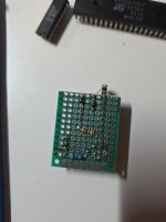
Thanks! I went for a socket adapter and am now waiting for the glue to dry. When it's done, do I still need to remove ROMs and RAMs in case of one such NOP generating 6502 compared to the ROM socketed type?
The value is not too important, as long as it is not too high or too low. Sounds like the story of goldilocks and the three bears!
This seems to be the standard reply when I ask about the value of pull-up resistors :)
 
Back
Top