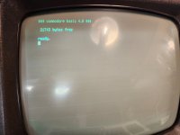
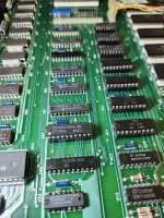
Absolutely! I'm tempted to pull the socket and make sure I didn't mess anything up. I'm usually pretty confident, but I also did the CPU socket (wouldn't work after the RAM/ROM board was inserted, and I lifted a pad on the CPU socket, so now I'm questioning my earlier work. (On the CPU socket, those white sockets are a b*tch. Part of the contact lays on TOP of the board, and you sometimes can't get it unstuck.)
They are not really a B*tch, if you understand them & take the time to test them. (it sounds like a remark from Women's Lib)
Those white sockets are known as single wipe types, because, when the IC pin goes into the socket, the metal claw on the socket only presses up against one flat face of the IC pin. Regrettably, the other face of the IC pin presses against plastic.
On the other hand, "dual wipe" sockets, have have a claw system that presses up against both of the flat faces of the IC pin. Improving the chances of a good connection.
Still, in the case of the single wipe white socket, they can still be ok of the IC pins on their outer surfaces are clean.
I have a PET still with single wipe original sockets & it is ok.
But, I have checked each socket receptacle, with a pin taken from a defunct IC and soldered to a small wire handle, so that I could confirm that each socket hole has a reasonable physical tension against the IC pin.
If any adapters with a geometry of a pin, that is greater than a typical IC pin is plugged in (and this applied to all IC sockets single wipe, dual wipe, machined pin, then unfortunately these is a loss of physical tension when a genuine IC pin is plugged into the socket later and poor connections result.
One interesting curio about the white single wipe IC sockets in the PET, is that you can lift off the plastic shroud. Then you have access to each socket, pin 1 by one if you need to replace them or remove them and fit a dual wipe socket instead.
") ...
...